HCPL3700 Fairchild Semiconductor, HCPL3700 Datasheet - Page 2
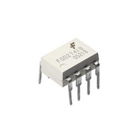
HCPL3700
Manufacturer Part Number
HCPL3700
Description
Logic Output Optocouplers AC/DC To Logic Interface
Manufacturer
Fairchild Semiconductor
Datasheet
1.HCPL3700.pdf
(11 pages)
Specifications of HCPL3700
Fall Time
400 ns
Logic Gate Type
Darlington Configuration
Rise Time
400 ns
Configuration
1 Channel
Isolation Voltage
2500 Vrms
Output Type
Open Collector
Maximum Propagation Delay Time
40000 ns
Maximum Forward Diode Voltage
0.65 V
Maximum Forward Diode Current
4.4 mA
Maximum Continuous Output Current
30 mA
Maximum Power Dissipation
210 mW
Maximum Operating Temperature
+ 70 C
Minimum Operating Temperature
0 C
Package / Case
DIP-8
Lead Free Status / RoHS Status
Lead free / RoHS Compliant
Other names
HCPL3700_NL
Available stocks
Company
Part Number
Manufacturer
Quantity
Price
Company:

Part Number:
HCPL3700
Manufacturer:
AGILENT
Quantity:
20 000
Part Number:
HCPL3700
Manufacturer:
QTC
Quantity:
20 000
Part Number:
HCPL3700SD
Manufacturer:
FAIRCHILD/仙童
Quantity:
20 000


©2005 Fairchild Semiconductor Corporation
HCPL3700 Rev. 1.0.3
Absolute Maximum Ratings
Stresses exceeding the absolute maximum ratings may damage the device. The device may not function or be
operable above the recommended operating conditions and stressing the parts to these levels is not recommended.
In addition, extended exposure to stresses above the recommended operating conditions may affect device reliability.
The absolute maximum ratings are stress ratings only.
Notes:
1. Derate linearly above 70°C free-air temperature at a rate of 1.8 mW/°C.
2. Derate linearly above 70°C free-air temperature at a rate of 2.5 mW/°C.
3. Derate linearly above 70°C free-air temperature at a rate of 0.6 mA/°C.
4. Derate linearly above 70°C free-air temperature at a rate of 1.9 mW/°C.
Recommended Operating Conditions
The Recommended Operating Conditions table defines the conditions for actual device operation. Recommended
operating conditions are specified to ensure optimal performance to the datasheet specifications. Fairchild does not
recommend exceeding them or designing to absolute maximum ratings.
EMITTER
DETECTOR
Symbol
Symbol
T
T
T
V
V
P
V
P
OPR
P
V
STG
I
SOL
I
T
IN
CC
O
IN
IN
O
CC
O
f
T
A
Storage Temperature
Operating Temperature
Lead Solder Temperature
Input Current
Input Voltage (Pins 2-3)
Input Power Dissipation
Total Package Power Dissipation
Output Current (Average)
Supply Voltage (Pins 8-5)
Output Voltage (Pins 6-5)
Output Power Dissipation
Supply Voltage
Operating Temperature
Operating Frequency
Parameter
(No derating required up to 70°C)
Average
Surge, 3ms, 120Hz Pulse Rate
Transient, 10µs, 120Hz Pulse Rate
(1)
(3)
(4)
Parameter
(2)
2
Min.
2
0
0
Max.
260 for 10 sec
18
70
-55 to +125
4
-0.5 (Max.)
140 (Max.)
500 (Max.)
230 (Max.)
305 (Max.)
210 (Max.)
-40 to +85
50 (Max.)
30 (Max.)
-0.5 to 20
-0.5 to 20
Value
www.fairchildsemi.com
Units
kHz
°C
Units
V
mW
mW
mW
mA
mA
°C
°C
°C
V
V
V
Related parts for HCPL3700
Image
Part Number
Description
Manufacturer
Datasheet
Request
R

Part Number:
Description:
Fairchild Semiconductor [IGBT MODULE]
Manufacturer:
Fairchild Semiconductor
Datasheet:

Part Number:
Description:
Discrete Semiconductor Modules
Manufacturer:
Fairchild Semiconductor
Part Number:
Description:
Discrete Semiconductor Modules
Manufacturer:
Fairchild Semiconductor
Part Number:
Description:
This N-Channel MOSFET is produced using Fairchild Semiconductor’s advanced Power Trench® process
Manufacturer:
Fairchild Semiconductor
Datasheet:
Part Number:
Description:
This N-Channel MOSFET is produced using Fairchild Semiconductor’s advanced Power Trench® process
Manufacturer:
Fairchild Semiconductor
Datasheet:
Part Number:
Description:
This N-Channel MOSFET is produced using Fairchild Semiconductor’s advanced PowerTrench® process
Manufacturer:
Fairchild Semiconductor
Datasheet:
Part Number:
Description:
This N-Channel MOSFET is produced using Fairchild Semiconductor’s advanced PowerTrench® process
Manufacturer:
Fairchild Semiconductor
Datasheet:
Part Number:
Description:
This N-Channel MOSFET is produced using Fairchild Semiconductor’s advanced Power Trench® process
Manufacturer:
Fairchild Semiconductor
Datasheet:
Part Number:
Description:
This N-Channel logic Level MOSFETs are produced using Fairchild Semiconductor‘s advanced Power Trench® process that has been special tailored to minimize the on-state resistance and yet maintain superior switching performance
Manufacturer:
Fairchild Semiconductor
Datasheet:
Part Number:
Description:
This N-Channel MOSFET is produced using Fairchild Semiconductor’s advanced Power Trench® process
Manufacturer:
Fairchild Semiconductor
Datasheet:
Part Number:
Description:
This N-Channel SyncFET™ is produced using Fairchild Semiconductor’s advanced PowerTrench® process
Manufacturer:
Fairchild Semiconductor
Datasheet:
Part Number:
Description:
This N-Channel SyncFET™ is produced using Fairchild Semiconductor’s advanced PowerTrench® process
Manufacturer:
Fairchild Semiconductor
Datasheet:
Part Number:
Description:
This N-Channel SyncFET™ is produced using Fairchild Semiconductor’s advanced PowerTrench® process
Manufacturer:
Fairchild Semiconductor
Datasheet:
Part Number:
Description:
This N-Channel logic Level MOSFETs are produced using Fairchild Semiconductor‘s advanced Power Trench® process that has been special tailored to minimize the on-state resistance and yet maintain superior switching performance
Manufacturer:
Fairchild Semiconductor
Datasheet:
Part Number:
Description:
This N-Channel MOSFET is produced using Fairchild Semiconductor’s advanced Power Trench® process that has been especially tailored to minimize the on-state resistance and yet maintain superior switching performance
Manufacturer:
Fairchild Semiconductor
Datasheet: