HCPL0701 Fairchild Semiconductor, HCPL0701 Datasheet - Page 4
HCPL0701
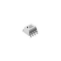
Manufacturer Part Number
HCPL0701
Description
High Speed Optocouplers Hi Gain Optocoupler 1Ch LC Darlington
Manufacturer
Fairchild Semiconductor
Datasheet
1.HCPL0701.pdf
(13 pages)
Specifications of HCPL0701
Input Type
DC
Isolation Voltage
2500 Vrms
Maximum Continuous Output Current
60 mA
Maximum Fall Time
60 us
Maximum Forward Diode Current
50 mA
Maximum Rise Time
25 us
Minimum Forward Diode Voltage
1 V
Output Device
Darlington With Base
Configuration
1 Channel
Current Transfer Ratio
5000 %
Maximum Baud Rate
100 KBps
Maximum Forward Diode Voltage
1.7 V
Maximum Reverse Diode Voltage
5 V
Maximum Input Diode Current
20 mA
Maximum Power Dissipation
100 mW
Maximum Operating Temperature
+ 85 C
Minimum Operating Temperature
- 40 C
Package / Case
SOIC-8 Narrow
Lead Free Status / RoHS Status
Lead free / RoHS Compliant
Other names
HCPL0701_NL
Available stocks
Company
Part Number
Manufacturer
Quantity
Price
Company:

Part Number:
HCPL0701
Manufacturer:
AGILENT
Quantity:
20 000
Part Number:
HCPL0701
Manufacturer:
FAIRCHILD/仙童
Quantity:
20 000
Company:
Part Number:
HCPL0701560E
Manufacturer:
AVAGO
Quantity:
2 702
Company:
Part Number:
HCPL0701R1
Manufacturer:
FAIRCHILD
Quantity:
3 500
Company:
Part Number:
HCPL0701R2
Manufacturer:
FAIRCHILD
Quantity:
3 500
Part Number:
HCPL0701R2
Manufacturer:
FAIRCHILD/仙童
Quantity:
20 000


©2003 Fairchild Semiconductor Corporation
HCPL0700, HCPL0701, HCPL0730, HCPL0731 Rev. 1.0.1
Electrical Characteristics
Switching Characteristics
*All typicals at T
Notes:
1. Current Transfer Ratio is defined as a ratio of output collector current, I
2. Pin 7 open. Use of a resistor between pins 5 and 7 will decrease gain and delay time.
3. Common mode transient immunity in logic high level is the maximum tolerable (positive) dV
4. Device is considered a two terminal device: Pins 1, 2, 3 and 4 are shorted together and Pins 5, 6, 7 and 8 are shorted
5. 2500 VAC RMS for 1 minute duration is equivalent to 3000 VAC RMS for 1 second duration.
Symbol
|CM
|CM
T
T
times 100%.
leading edge of the common mode pulse signal, V
(i.e., V
on the trailing edge of the common mode pulse signal, V
(i.e., V
together.
PHL
PLH
H
L
|
|
O
O
Propagation Delay
Time to Logic Low
(Note 2) (Fig. 14)
Propagation Delay
Time to Logic High
(Note 2) (Fig. 14)
Common Mode
Transient
Immunity at
Logic High
Common Mode
Transient
Immunity at
Logic Low
<0.8 V).
> 2.0V). Common mode transient immunity in logic low level is the maximum tolerable (negative) dV
Parameter
A
= 25°C
(V
R
R
R
R
R
R
I
T
(Note 3) (Fig. 15)
I
T
(Note 3) (Fig. 15)
CC
F
F
A
A
L
L
L
L
L
L
= 0mA, |V
= 1.6mA, |V
= 25°C, R
= 25°C, R
= 4.7k , I
= 270 , I
= 2.2 k , I
= 4.7 k , I
= 270 , I
= 2.2 k , I
(T
= 5V)
A
Test Conditions
= 0 to 70°C unless otherwise specified)
CM
L
L
F
F
F
F
F
F
CM
= 2.2k
= 2.2 k
= 0.5mA
= 12mA
= 12mA
| = 10 V
= 1.6mA
= 0.5mA
= 1.6mA
| = 10 V
T
T
T
T
T
T
A
A
A
A
A
A
CM
= 25°C
= 25°C
= 25°C
= 25°C
= 25°C
= 25°C
P-P
, to assure that the output will remain in a logic high state
P-P
4
,
CM
,
, to assure that the output will remain in a logic low state
HCPL0700/30/31
HCPL0700/30/31
HCPL0730/0731
HCPL0730/0731
HCPL0701/31
HCPL0701/31
HCPL0701
HCPL0731
HCPL0701
HCPL0731
HCPL0701
HCPL0731
HCPL0701
HCPL0731
HCPL0700
HCPL0700
HCPL0701
HCPL0731
HCPL0701
HCPL0731
Device
ALL
ALL
O
, to the forward LED input current, I
1,000
1,000
Min.
10,000
10,000
CM
Typ.*
0.3
0.4
1.6
1.6
12
3
5
1
2
7
/dt on the
Max. Unit
www.fairchildsemi.com
120
100
30
25
15
25
10
20
90
60
10
15
10
50
35
2
3
1
2
7
F
CM
,
V/µs
V/µs
µs
µs
/dt
Related parts for HCPL0701
Image
Part Number
Description
Manufacturer
Datasheet
Request
R

Part Number:
Description:
Fairchild Semiconductor [IGBT MODULE]
Manufacturer:
Fairchild Semiconductor
Datasheet:

Part Number:
Description:
Discrete Semiconductor Modules
Manufacturer:
Fairchild Semiconductor
Part Number:
Description:
Discrete Semiconductor Modules
Manufacturer:
Fairchild Semiconductor
Part Number:
Description:
This N-Channel MOSFET is produced using Fairchild Semiconductor’s advanced Power Trench® process
Manufacturer:
Fairchild Semiconductor
Datasheet:
Part Number:
Description:
This N-Channel MOSFET is produced using Fairchild Semiconductor’s advanced Power Trench® process
Manufacturer:
Fairchild Semiconductor
Datasheet:
Part Number:
Description:
This N-Channel MOSFET is produced using Fairchild Semiconductor’s advanced PowerTrench® process
Manufacturer:
Fairchild Semiconductor
Datasheet:
Part Number:
Description:
This N-Channel MOSFET is produced using Fairchild Semiconductor’s advanced PowerTrench® process
Manufacturer:
Fairchild Semiconductor
Datasheet:
Part Number:
Description:
This N-Channel MOSFET is produced using Fairchild Semiconductor’s advanced Power Trench® process
Manufacturer:
Fairchild Semiconductor
Datasheet:
Part Number:
Description:
This N-Channel logic Level MOSFETs are produced using Fairchild Semiconductor‘s advanced Power Trench® process that has been special tailored to minimize the on-state resistance and yet maintain superior switching performance
Manufacturer:
Fairchild Semiconductor
Datasheet:
Part Number:
Description:
This N-Channel MOSFET is produced using Fairchild Semiconductor’s advanced Power Trench® process
Manufacturer:
Fairchild Semiconductor
Datasheet:
Part Number:
Description:
This N-Channel SyncFET™ is produced using Fairchild Semiconductor’s advanced PowerTrench® process
Manufacturer:
Fairchild Semiconductor
Datasheet:
Part Number:
Description:
This N-Channel SyncFET™ is produced using Fairchild Semiconductor’s advanced PowerTrench® process
Manufacturer:
Fairchild Semiconductor
Datasheet:
Part Number:
Description:
This N-Channel SyncFET™ is produced using Fairchild Semiconductor’s advanced PowerTrench® process
Manufacturer:
Fairchild Semiconductor
Datasheet:
Part Number:
Description:
This N-Channel logic Level MOSFETs are produced using Fairchild Semiconductor‘s advanced Power Trench® process that has been special tailored to minimize the on-state resistance and yet maintain superior switching performance
Manufacturer:
Fairchild Semiconductor
Datasheet:
Part Number:
Description:
This N-Channel MOSFET is produced using Fairchild Semiconductor’s advanced Power Trench® process that has been especially tailored to minimize the on-state resistance and yet maintain superior switching performance
Manufacturer:
Fairchild Semiconductor
Datasheet: