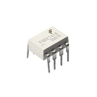
FOD3180 Fairchild Semiconductor, FOD3180 Datasheet - Page 2
FOD3180
Manufacturer Part Number
FOD3180
Description
High Speed Optocouplers MOSFET 2A OUT Gate Drvr Optocoupler
Manufacturer
Fairchild Semiconductor
Datasheet
1.FOD3180TV.pdf
(13 pages)
Specifications of FOD3180
Input Type
DC
Isolation Voltage
5000 Vrms
Minimum Forward Diode Voltage
1.2 V
Output Device
Transistor
Configuration
1 Channel
Maximum Forward Diode Voltage
1.8 V
Maximum Reverse Diode Voltage
5 V
Maximum Input Diode Current
25 mA
Maximum Power Dissipation
295 mW
Maximum Operating Temperature
+ 100 C
Minimum Operating Temperature
- 40 C
Package / Case
DIP-8
Number Of Elements
1
Output Type
Push-Pull
Forward Voltage
1.8V
Forward Current
25mA
Package Type
PDIP W
Operating Temp Range
-40C to 100C
Power Dissipation
295mW
Propagation Delay Time
200ns
Pin Count
8
Mounting
Through Hole
Reverse Breakdown Voltage
5V
Operating Temperature Classification
Industrial
Lead Free Status / RoHS Status
Lead free / RoHS Compliant
Available stocks
Company
Part Number
Manufacturer
Quantity
Price

Part Number:
FOD3180
Manufacturer:
FAIRCHILD/仙童
Quantity:
20 000
Part Number:
FOD3180S
Manufacturer:
FAIRCHILD/仙童
Quantity:
20 000
Part Number:
FOD3180SD
Manufacturer:
ON/安森美
Quantity:
20 000
Company:
Part Number:
FOD3180SDV
Manufacturer:
WILLAS
Quantity:
30 000
Part Number:
FOD3180SDV
Manufacturer:
ON/安森美
Quantity:
20 000
Part Number:
FOD3180SV
Manufacturer:
ON/FCS
Quantity:
20 000
Company:
Part Number:
FOD3180TV
Manufacturer:
Fairchild Semiconductor
Quantity:
1 969


©2005 Fairchild Semiconductor Corporation
FOD3180 Rev. 1.0.6
Absolute Maximum Ratings
Stresses exceeding the absolute maximum ratings may damage the device. The device may not function or be
operable above the recommended operating conditions and stressing the parts to these levels is not recommended.
In addition, extended exposure to stresses above the recommended operating conditions may affect device reliability.
The absolute maximum ratings are stress ratings only.
Recommended Operating Conditions
The Recommended Operating Conditions table defines the conditions for actual device operation. Recommended
operating conditions are specified to ensure optimal performance to the datasheet specifications. Fairchild does not
recommend exceeding them or designing to absolute maximum ratings.
V
V
I
Symbol
I
Symbol
V
OH(PEAK)
OL(PEAK)
I
CC
CC
V
I
I
F(TRAN)
O(PEAK)
I
T
F(AVG)
T
T
F(tr, tf)
F(ON)
F(OFF)
P
OPR
V
P
STG
T
SOL
– V
– V
R
O
D
J
EE
EE
Parameter
Storage Temperature
Operating Temperature
Junction Temperature
Lead Solder Temperature
Average Input Current
LED Current Minimum Rate of Rise/Fall
Peak Transient Input Current (<1µs pulse width, 300pps)
Reverse Input Voltage
“High” Peak Output Current
“Low” Peak Output Current
Supply Voltage
Output Voltage
Output Power Dissipation
Total Power Dissipation
Parameter
Power Supply
Input Current (ON)
Input Voltage (OFF)
(T
A
= 25°C unless otherwise specified)
(1)
(5)
(4)
(2)
(2)
2
260 for 10 sec.
-40 to +125
-40 to +100
-40 to +125
-3.0 to 0.8
-0.5 to 25
0 to V
10 to 20
10 to 16
Value
Value
250
250
295
1.0
2.5
2.5
25
5
CC
www.fairchildsemi.com
Units
Units
mW
mW
mA
mA
°C
°C
°C
°C
ns
A
V
A
A
V
V
V
V
Related parts for FOD3180
Image
Part Number
Description
Manufacturer
Datasheet
Request
R

Part Number:
Description:
Fairchild Semiconductor [IGBT MODULE]
Manufacturer:
Fairchild Semiconductor
Datasheet:

Part Number:
Description:
Discrete Semiconductor Modules
Manufacturer:
Fairchild Semiconductor
Part Number:
Description:
Discrete Semiconductor Modules
Manufacturer:
Fairchild Semiconductor
Part Number:
Description:
This N-Channel MOSFET is produced using Fairchild Semiconductor’s advanced Power Trench® process
Manufacturer:
Fairchild Semiconductor
Datasheet:
Part Number:
Description:
This N-Channel MOSFET is produced using Fairchild Semiconductor’s advanced Power Trench® process
Manufacturer:
Fairchild Semiconductor
Datasheet:
Part Number:
Description:
This N-Channel MOSFET is produced using Fairchild Semiconductor’s advanced PowerTrench® process
Manufacturer:
Fairchild Semiconductor
Datasheet:
Part Number:
Description:
This N-Channel MOSFET is produced using Fairchild Semiconductor’s advanced PowerTrench® process
Manufacturer:
Fairchild Semiconductor
Datasheet:
Part Number:
Description:
This N-Channel MOSFET is produced using Fairchild Semiconductor’s advanced Power Trench® process
Manufacturer:
Fairchild Semiconductor
Datasheet:
Part Number:
Description:
This N-Channel logic Level MOSFETs are produced using Fairchild Semiconductor‘s advanced Power Trench® process that has been special tailored to minimize the on-state resistance and yet maintain superior switching performance
Manufacturer:
Fairchild Semiconductor
Datasheet:
Part Number:
Description:
This N-Channel MOSFET is produced using Fairchild Semiconductor’s advanced Power Trench® process
Manufacturer:
Fairchild Semiconductor
Datasheet:
Part Number:
Description:
This N-Channel SyncFET™ is produced using Fairchild Semiconductor’s advanced PowerTrench® process
Manufacturer:
Fairchild Semiconductor
Datasheet:
Part Number:
Description:
This N-Channel SyncFET™ is produced using Fairchild Semiconductor’s advanced PowerTrench® process
Manufacturer:
Fairchild Semiconductor
Datasheet:
Part Number:
Description:
This N-Channel SyncFET™ is produced using Fairchild Semiconductor’s advanced PowerTrench® process
Manufacturer:
Fairchild Semiconductor
Datasheet:
Part Number:
Description:
This N-Channel logic Level MOSFETs are produced using Fairchild Semiconductor‘s advanced Power Trench® process that has been special tailored to minimize the on-state resistance and yet maintain superior switching performance
Manufacturer:
Fairchild Semiconductor
Datasheet:
Part Number:
Description:
This N-Channel MOSFET is produced using Fairchild Semiconductor’s advanced Power Trench® process that has been especially tailored to minimize the on-state resistance and yet maintain superior switching performance
Manufacturer:
Fairchild Semiconductor
Datasheet: