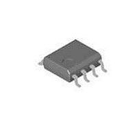
FOD3180S Fairchild Semiconductor, FOD3180S Datasheet - Page 5

FOD3180S
Manufacturer Part Number
FOD3180S
Description
High Speed Optocouplers 2A IGBT/FET GTE DRV OPTOCOUPLER
Manufacturer
Fairchild Semiconductor
Datasheet
1.FOD3180TV.pdf
(13 pages)
Specifications of FOD3180S
Input Type
DC
Isolation Voltage
5000 Vrms
Minimum Forward Diode Voltage
1.2 V
Output Device
Transistor
Configuration
1 Channel
Maximum Forward Diode Voltage
1.8 V
Maximum Reverse Diode Voltage
5 V
Maximum Input Diode Current
25 mA
Maximum Power Dissipation
295 mW
Maximum Operating Temperature
+ 100 C
Minimum Operating Temperature
- 40 C
Package / Case
SMD-8
Lead Free Status / RoHS Status
Lead free / RoHS Compliant
Available stocks
Company
Part Number
Manufacturer
Quantity
Price
Part Number:
FOD3180S
Manufacturer:
FAIRCHILD/仙童
Quantity:
20 000
Part Number:
FOD3180SD
Manufacturer:
ON/安森美
Quantity:
20 000
Company:
Part Number:
FOD3180SDV
Manufacturer:
WILLAS
Quantity:
30 000
Part Number:
FOD3180SDV
Manufacturer:
ON/安森美
Quantity:
20 000
Part Number:
FOD3180SV
Manufacturer:
ON/FCS
Quantity:
20 000
©2005 Fairchild Semiconductor Corporation
FOD3180 Rev. 1.0.6
Notes:
1. Derate linearly above +70°C free air temperature at a rate of 0.3mA/°C.
2. The output currents I
3. The output currents I
4. Derate linearly above +87°C, free air temperature at the rate of 0.77mW/°C. Refer to Figure 12.
5. No derating required across operating temperature range.
6. In this test, V
7. Maximum pulse width = 1ms, maximum duty cycle = 20%.
8. t
9. PWD is defined as | t
10. The difference between t
11. Pin 1 and 4 need to be connected to LED common.
12. Common mode transient immunity in the high state is the maximum tolerable dV
13. Common mode transient immunity in a low state is the maximum tolerable dV
14. In accordance with UL 1577, each optocoupler is proof tested by applying an insulation test voltage > 6000Vrms,
15. Device considered a two-terminal device: pins on input side shorted together and pins on output side shorted
frequency = 8kHz, 50% DF.
frequency = 8kHz, 50% DF.
as I
falling edge of the V
pulse to the 50% level of the rising edge of the V
V
V
60Hz for 1 second (leakage detection current limit I
together.
PHL
CM
CM
OH
, to assure that the output will remain in a low state (i.e. V
propagation delay is measured from the 50% level on the falling edge of the input pulse to the 50% level of the
to assure that the output will remain in the high state (i.e. V
approaches zero amps.
OH
is measured with a dc load current of 100mA. When driving capacitive load V
O
OH
OH
PHL
signal. t
and I
and I
PHL
– t
PLH
and t
OL
OL
PLH
| for any given device.
are specified with a capacitive current limited load = (3 x 0.01µF) + 0.5 ,
are specified with a capacitive current limited load = (3 x 0.01µF) + 8.5 ,
propagation delay is measured from the 50% level on the rising edge of the input
PLH
between any two FOD3180 parts under same test conditions.
O
signal.
I-O
< 5µA).
5
O
< 1.0V).
O
> 10.0V).
CM
CM
/dt of the common mode pulse,
/dt of the common mode pulse
OH
will approach V
www.fairchildsemi.com
CC


