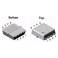
FDMC86102 Fairchild Semiconductor, FDMC86102 Datasheet - Page 2

FDMC86102
Manufacturer Part Number
FDMC86102
Description
MOSFET N-CH 100V 8-MLP
Manufacturer
Fairchild Semiconductor
Series
PowerTrench®r
Datasheet
1.FDMC86102.pdf
(7 pages)
Specifications of FDMC86102
Fet Type
MOSFET N-Channel, Metal Oxide
Fet Feature
Logic Level Gate
Rds On (max) @ Id, Vgs
24 mOhm @ 7A, 10V
Drain To Source Voltage (vdss)
100V
Current - Continuous Drain (id) @ 25° C
7A
Vgs(th) (max) @ Id
4V @ 250µA
Gate Charge (qg) @ Vgs
18nC @ 10V
Input Capacitance (ciss) @ Vds
965pF @ 50V
Power - Max
2.3W
Mounting Type
Surface Mount
Package / Case
8-MLP, Power33
Configuration
Single
Transistor Polarity
N-Channel
Resistance Drain-source Rds (on)
32.8 mOhms
Forward Transconductance Gfs (max / Min)
19 S
Drain-source Breakdown Voltage
100 V
Gate-source Breakdown Voltage
+/- 20 V
Continuous Drain Current
20 A
Power Dissipation
41 W
Maximum Operating Temperature
+ 150 C
Mounting Style
SMD/SMT
Minimum Operating Temperature
- 55 C
Lead Free Status / RoHS Status
Lead free / RoHS Compliant
Available stocks
Company
Part Number
Manufacturer
Quantity
Price
Company:
Part Number:
FDMC86102
Manufacturer:
IR
Quantity:
21 000
Part Number:
FDMC86102
Manufacturer:
FAIRCHILD/仙童
Quantity:
20 000
Part Number:
FDMC86102L
Manufacturer:
ON/安森美
Quantity:
20 000
Part Number:
FDMC86102LZ
Manufacturer:
FAIRCHILD/仙童
Quantity:
20 000
FDMC86102 Rev.C
Electrical Characteristics
Off Characteristics
On Characteristics
Dynamic Characteristics
Switching Characteristics
Drain-Source Diode Characteristics
NOTES:
1. R
2. Pulse Test: Pulse Width < 300 µs, Duty cycle < 2.0 %.
3. Starting T
BV
∆BV
I
I
V
r
g
C
C
C
R
t
t
t
t
Q
Q
Q
V
t
Q
DSS
GSS
∆V
d(on)
r
d(off)
f
rr
DS(on)
FS
GS(th)
SD
the user's board design.
∆T
∆T
iss
oss
rss
g
g(TOT)
gs
gd
rr
Symbol
θJA
DSS
GS(th)
DSS
J
J
is determined with the device mounted on a 1in
J
= 25
o
Drain to Source Breakdown Voltage
Breakdown Voltage Temperature
Coefficient
Zero Gate Voltage Drain Current
Gate to Source Leakage Current
Gate to Source Threshold Voltage
Gate to Source Threshold Voltage
Temperature Coefficient
Static Drain to Source On Resistance
Forward Transconductance
Input Capacitance
Output Capacitance
Reverse Transfer Capacitance
Gate Resistance
Turn-On Delay Time
Rise Time
Turn-Off Delay Time
Fall Time
Total Gate Charge
Total Gate Charge
Total Gate Charge
Gate to Drain “Miller” Charge
Source to Drain Diode Forward Voltage
Reverse Recovery Time
Reverse Recovery Charge
C; N-ch: L = 1 mH, I
AS
Parameter
= 12 A, V
DD
a.
2
T
53 °C/W when mounted on a
1 in
= 90 V, V
pad 2 oz copper pad on a 1.5 x 1.5 in. board of FR-4 material. R
J
= 25 °C unless otherwise noted
2
pad of 2 oz copper
GS
= 10 V.
I
I
V
V
V
I
V
V
V
V
D
D
D
V
V
V
V
V
f = 1 MHz
V
V
I
DS
GS
GS
GS
GS
GS
DD
F
DS
DD
GS
GS
GS
= 250 µA, V
= 250 µA, referenced to 25 °C
GS
GS
= 250 µA, referenced to 25 °C
= 7 A, di/dt = 100 A/µs
= 80 V, V
= ±20 V, V
= V
= 10 V, I
= 6 V, I
= 10 V, I
= 10 V, I
= 50 V, I
= 10 V, R
= 0 V to 10 V
= 0 V to 5 V
= 50 V, V
= 0 V, I
= 0 V, I
2
DS
Test Conditions
, I
D
S
S
D
D
D
D
D
GS
GS
= 5 A
= 7 A
= 2 A
GS
GEN
DS
= 250 µA
= 7 A
= 7 A, T
= 7 A
= 7 A,
= 0 V
= 0 V
= 0 V,
= 0 V
= 6 Ω
V
I
D
DD
= 7 A
J
= 50 V
= 125 °C
(Note 2)
(Note 2)
θJC
is guaranteed by design while R
b.
125 °C/W when mounted on
a minimum pad of 2 oz copper
Min
100
2.0
0.81
0.75
19.4
26.8
32.8
Typ
725
175
3.7
3.6
3.1
44
40
0.5
14
13
19
15
69
-9
8
4
4
8
±100
Max
θCA
1.3
1.2
965
235
70
65
www.fairchildsemi.com
4.0
17
10
25
10
18
11
24
38
41
25
1
is determined by
mV/°C
mV/°C
Units
mΩ
nC
nC
nC
nC
nC
µA
nA
pF
pF
pF
ns
ns
ns
ns
ns
Ω
V
V
V
S


