GP1A51HRJ00F Sharp Microelectronics, GP1A51HRJ00F Datasheet - Page 4
GP1A51HRJ00F
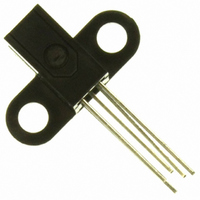
Manufacturer Part Number
GP1A51HRJ00F
Description
PHOTOINTER OPIC SLOT 3.0MM PCB
Manufacturer
Sharp Microelectronics
Series
OPIC™r
Datasheet
1.GP1A51HRJ00F.pdf
(12 pages)
Specifications of GP1A51HRJ00F
Package / Case
PCB Mount
Sensing Distance
0.118" (3mm)
Sensing Method
Transmissive
Output Configuration
Pull-Up Resistor, Buffer
Mounting Type
Through Hole
Current - Supply
1.7mA
Voltage - Supply
4.5 V ~ 17 V
Response Time
1µs, 0.05µs
No. Of Channels
1
Input Current
5mA
Output Voltage
4.9V
Opto Case Style
Through Hole
No. Of Pins
5
Operating Temperature Range
-25°C To +85°C
Output Type
Transistor
Maximum Reverse Voltage (emitter)
6 V
Slot Width
3 mm
Aperture Width
0.5 mm
Output Device
Photologic, Pull up
Power Dissipation
250 mW
Maximum Fall Time
500 ns
Maximum Operating Temperature
+ 85 C
Maximum Rise Time
500 ns
Minimum Operating Temperature
- 25 C
Optocoupler Output Type
Transistor
Svhc
No SVHC (15-Dec-2010)
Rohs Compliant
Yes
Lead Free Status / RoHS Status
Lead free / RoHS Compliant
Lead Free Status / RoHS Status
Lead free / RoHS Compliant
Other names
425-1949-5
Available stocks
Company
Part Number
Manufacturer
Quantity
Price


■ Absolute Maximum Ratings
∗
∗
∗
■ Electro-optical Characteristics
∗
∗
∗
1 The derating factors of absolute maximum ratings due to ambient temperature are shown in Fig. 1, 2, 3
2 Pulse width ≤ 100 μ s, Duty ratio = 0.01
3 For 5s or less
4 I
5 I
6 Test circuit for response time is shown in Fig.12.
Output
Output
∗ 3
Transfer
teristics
charac-
Input
Input
FLH
FHL
Operating temperature
Storage temperature
Soldering temperature
represents forward current when output goes from "Low" to "High".
represents forward current when output goes from "High" to "Low".
6 ∗
∗ 1
∗ 1, 2
∗ 4
∗ 5
"Low → High" threshold input current
Hysteresis
Forward voltage
Reverse current
Operating supply voltage
Low level output voltage
High level output voltage
Low level supply current
High level supply current
Forward current
Peak forward current
Reverse voltage
Power dissipation
Supply voltage
Output current
Power dissipation
"Low → High" Propagation delay time
"High → Low" Propagation delay time
Rise time
Fall time
Parameter
Parameter
Symbol
V
T
T
T
I
V
P
I
I
FM
P
opr
CC
O
stg
sol
F
O
R
I
Symbol
FHL
V
V
I
I
V
I
t
t
V
CCH
PLH
PHL
CCL
FLH
I
t
t
OH
/I
R
CC
OL
r
f
− 40 to + 100
F
− 0.5 to + 17
− 25 to + 85
FLH
Rating
250
260
50
75
50
1
6
V
V
CC
(T
CC
4
= 5V, I
a
= 5V, I
V
V
= 25˚C)
Unit
mW
mW
mA
mA
˚C
˚C
˚C
V
V
A
CC
V
CC
Condition
CC
= 5V, I
= 5V, I
V
V
I
F
V
F
= 5mA, R
= 5V, I
OL
CC
CC
= 5mA
R
= 3V
−
= 16mA, I
= 5V
= 5V
F
F
= 5mA
= 5mA
F
= 0
L
= 280 Ω
F
= 0
MIN.
0.55
4.5
4.9
−
−
−
−
−
−
−
−
−
−
TYP.
0.15
0.75
0.05
1.1
1.7
0.7
0.1
−
−
−
1
3
5
Sheet No.: D3-A03601EN
GP1A51HRJ00F
MAX.
0.95
1.4
0.4
3.8
2.2
0.5
0.5
10
17
15
−
5
9
(T
a
= 25˚C)
Unit
mA
mA
mA
μ A
μ s
V
V
V
V
−
Related parts for GP1A51HRJ00F
Image
Part Number
Description
Manufacturer
Datasheet
Request
R

Part Number:
Description:
PHOTOINTER OPIC SLOT 3.0MM PCB
Manufacturer:
Sharp Microelectronics
Datasheet:

Part Number:
Description:
IC FLASH 32MBIT 110NS 56SSOP
Manufacturer:
Sharp Microelectronics
Datasheet:

Part Number:
Description:
IC FLASH 16MBIT 100NS 56TSOP
Manufacturer:
Sharp Microelectronics
Datasheet:
Part Number:
Description:
IC FLASH 64MBIT 120NS 56TSOP
Manufacturer:
Sharp Microelectronics
Datasheet:

Part Number:
Description:
IC FLASH 16MBIT 90NS 48TSOP
Manufacturer:
Sharp Microelectronics
Datasheet:
Part Number:
Description:
IC SRAM 16KBIT 100NS 24DIP
Manufacturer:
Sharp Microelectronics
Datasheet:
Part Number:
Description:
IC SRAM 16KBIT 100NS 24SOP
Manufacturer:
Sharp Microelectronics
Datasheet:
Part Number:
Description:
IC SRAM 64KBIT 100NS 28DIP
Manufacturer:
Sharp Microelectronics
Datasheet:
Part Number:
Description:
IC SRAM 64KBIT 100NS 28SOP
Manufacturer:
Sharp Microelectronics
Datasheet:
Part Number:
Description:
IC SRAM 64KBIT 100NS 28SOP
Manufacturer:
Sharp Microelectronics
Datasheet:
Part Number:
Description:
IC SRAM 256KBIT 70NS 28DIP
Manufacturer:
Sharp Microelectronics
Datasheet:
Part Number:
Description:
IC FLASH 8MBIT 90NS 48TSOP
Manufacturer:
Sharp Microelectronics
Datasheet:
Part Number:
Description:
IC FLASH 8MBIT 85NS 40TSOP
Manufacturer:
Sharp Microelectronics
Datasheet:
Part Number:
Description:
IC FLASH 8MBIT 85NS 40TSOP
Manufacturer:
Sharp Microelectronics
Datasheet:
Part Number:
Description:
IC FLASH 16MBIT 90NS 48TSOP
Manufacturer:
Sharp Microelectronics
Datasheet: