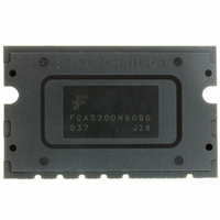
FCAS20DN60BB Fairchild Semiconductor, FCAS20DN60BB Datasheet

FCAS20DN60BB
Specifications of FCAS20DN60BB
Available stocks
Related parts for FCAS20DN60BB
FCAS20DN60BB Summary of contents
Page 1
... The high speed built-in HVIC provides opto- coupler-less IGBT gate driving capability that further reduce the overall size of the system. In addition the incorporated HVIC facilitates the use of single-supply drive topology enabling the FCAS20DN60BB to be driven by only one drive supply voltage without negative bias. Figure 1. 1 January 2008 www ...
Page 2
... Control supply circuit under-voltage (UV) protection • Fault signaling: Corresponding fault (Low-side supply) • Input interface: 5V CMOS/LSTTL compatible, Schmitt trigger input Pin Configuration #1 #1 (1)V- (1)V- ((3)U-) ((3)U-) ((2)V-) ((2)V-) (4)U- (4)U- FCAS20DN60BB Rev. A (5)V (5)V /V+ /V+ (7)Vth (7)Vth (9)V (9)V /U+ /U+ (11)IN (11)IN S(V) ...
Page 3
... COM FCAS20DN60BB Rev. A Pin Description Output for V- Leg Output for V- Leg Output for U- Leg Output for U- Leg Output for V+ Leg / High-side Bias Voltage Ground for V-phase IGBT Gate Driving High-side Bias Voltage for V-phase IGBT Gate Driving Thermistor Output Signal Input for V-phase High-side IGBT ...
Page 4
... Internal Equivalent Circuit and Input/Output Pins (10) V (11) IN (6) V (8) IN (12) C (13) C (14) V (16) IN (15) IN (17) V (18) COM (7) V FCAS20DN60BB Rev. A B(U) VCC VB (UH) IN(UH) OUT COM VS B(V) VCC VB (VH) IN(VH) OUT COM OUT(UL) Csc FOD Cfod FO Vfo (UL) IN(UL) (VL) IN(VL) CC VCC OUT(VL) ...
Page 5
... R Junction to Case Thermal th(j-c)Q Resistance R th(j-c)F Note: 1. For the measurement point of case temperature (T Package Marking & Ordering Information Device Marking Device FCAS20DN60BB FCAS20DN60BB FCAS20DN60BB Rev 25°C, Unless Otherwise Specified) J Conditions Applied between 25° 25°C, Under 1ms Pulse Width 25°C per One IGBT ...
Page 6
... ON t C(ON) t OFF t C(OFF Collector - Emitter CES Leakage Current Note and t include the propagation delay time of the internal drive IC OFF For the detailed information, please see Figure FCAS20DN60BB Rev 25°C, Unless Otherwise Specified) J Conditions 15V I = 15A 15A 300V 15V 20A ↔ 5V, Inductive Load ...
Page 7
... BS f PWM Input Signal PWM V Input ON Voltage IN(ON) V Input OFF Voltage IN(OFF) Bootstrap Diode Part Symbol Parameter V Maixmum Repetitive Reveres Voltage RRM I Forward Current F I Forward Current (Peak Reverse Recovery Time J FCAS20DN60BB Rev 25°C, Unless Otherwise Specified) J Conditions V = 15V V - COM ( 15V ( 0V, V Circuit: 4.7kΩ ...
Page 8
... Mechanical Characteristics and Ratings Parameter Mounting Torque Mounting Screw - M3 Surface Flatness Note Figure 5. Weight FCAS20DN60BB Rev. A Conditions Figure 5. Flatness Measurement Position 8 Limits Units Min. Typ. Max. 5.17 6.29 7.30 Kg•cm 0.51 0.62 0.72 N• 14 www.fairchildsemi.com ...
Page 9
... Control supply voltage rises: After the voltage reaches Normal operation: IGBT ON and carrying current Under voltage detection (UV BSD b4 : IGBT OFF in spite of control input condition, but there is no fault output signal Under voltage reset (UV ) BSR b6 : Normal operation: IGBT ON and carrying current FCAS20DN60BB Rev. A RESET SET UV CCR a1 UV CCD a3 ...
Page 10
... Fault output timer operation starts: The pulse width of the fault output signal is set by the external capacitor Input “L” : IGBT OFF state Input “H”: IGBT ON state, but during the active period of fault output the IGBT doesn’t turn ON IGBT OFF state Fig. 8. Short-Circuit Current Protection (Low-side Operation only) 100 FCAS20DN60BB Rev tio lta ...
Page 11
... This Value depend on PWM Control Algorithm 15V-Line 18uF 1000uF Note: 1) The ceramic capacitor placed between V -COM should be over 1uF and mounted as close to the pins of the SPM as possible. CC Figure 11. Recommended Bootstrap Operation Circuit and Parameters FCAS20DN60BB Rev. A 5V-Line Ω 4.7k Ω 100 ...
Page 12
... Gating V Gating line Fault Temp sense FCAS20DN60BB Rev. A (10) V B(U) VCC VB (11) IN (UH) OUT IN(UH) COM VS (6) V B(V) VCC VB (8) IN (VH) IN(VH) OUT COM VS VS (12 OUT(UL) Csc (13) C FOD Cfod (14 Vfo (16) IN (UL) IN(UL) (15) IN (VL) IN(VL) 15V line (17 VCC (18) COM OUT(VL) 5V line ...
Page 13
... Detailed Package Outline Drawings PACKAGE CENTER (3.22) 2-1.50 ±0.10 2-MAX1.60 20-0.60 ±0. 18.155 FCAS20DN60BB Rev. A 45.00 ±0.20 42.00 ±0.10 PACKAGE CENTER 18-MAX0. ±0.50 13 5.50 ±0.20 3.60 +0.10 0.50 3.10 ±0.30 -0.05 5.00 ±0.30 www.fairchildsemi.com ...
Page 14
... TRADEMARKS The following includes registered and unregistered trademarks and service marks, owned by Fairchild Semiconductor and/or its global subsidiaries, and is not intended exhaustive list of all such trademarks. ® ACEx Build it Now™ CorePLUS™ CROSSVOLT™ CTL™ Current Transfer Logic™ ...


