FSB50325S Fairchild Semiconductor, FSB50325S Datasheet
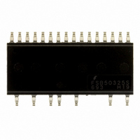
IC SMART POWER MOD 1.5A SPM23-BA

FSB50325S

Manufacturer Part Number
FSB50325S
Description
IC SMART POWER MOD 1.5A SPM23-BA
Manufacturer
Fairchild Semiconductor
Series
SPM™r
Type
FETr
Datasheet

Specifications of FSB50325S

Configuration
3 Phase
Current
1.5A
Voltage
250V
Voltage - Isolation
1500Vrms
Package / Case
SPM23BA
Input Voltage
250V
Output Current
3A
Power Dissipation Pd
10W
Supply Voltage Range
13.5V To 16.5V
No. Of Pins
23
Termination Type
SMD
Continuous Drain Current Id
1.5A
Supply Voltage Min
150V
Rohs Compliant
Yes
Filter Terminals
SMD
Current, Idm Pulse
3A
Lead Free Status / RoHS Status
Lead free / RoHS Compliant
Other names
FSB50325S
FSB50325STR
©2007 Fairchild Semiconductor Corporation
FSB50325S Rev. B
FSB50325S
Smart Power Module (SPM
Features
• 250V 1.5A 3-phase FRFET inverter including high voltage
• 3 divided negative dc-link terminals for inverter current sens-
• HVIC for gate driving and undervoltage protection
• 3/5V CMOS/TTL compatible, active-high interface
• Optimized for low electromagnetic interference
• Isolation voltage rating of 1500Vrms for 1min.
• Surface mounted device package
• Moisture Sensitive Level (MSL) 3
Absolute Maximum Ratings
Symbol
integrated circuit (HVIC)
ing applications
T
R
V
V
V
I
I
V
I
V
P
D25
D80
T
STG
DP
θJC
ISO
CC
PN
BS
IN
D
J
DC Link Input Voltage,
Drain-source Voltage of each FRFET
Each FRFET Drain Current, Continuous
Each FRFET Drain Current, Peak
Maximum Power Dissipation
Control Supply Voltage
High-side Bias Voltage
Input Signal Voltage
Operating Junction Temperature
Storage Temperature
Junction to Case Thermal Resistance
Isolation Voltage
Parameter
®
)
T
T
T
T
Applied between V
Applied between V
Applied between IN and COM
Each FRFET under inverter operating con-
dition (Note 1)
60Hz, Sinusoidal, 1 minute, Connection pins
to heatsink
C
C
C
C
= 25°C
= 80°C
= 25°C, PW < 100μs
= 25°C, Each FRFET
1
General Description
FRFET technology as a compact inverter solution for small
power motor drive applications such as fan motors and water
suppliers. It is composed of 6 fast-recovery MOSFET (FRFET),
and 3 half-bridge HVICs for FRFET gate driving. FSB50325S
provides low electromagnetic interference (EMI) characteristics
with optimized switching speed. Moreover, since it employs
FRFET as a power switch, it has much better ruggedness and
larger safe operation area (SOA) than that of an IGBT-based
power module or one-chip solution. The package is optimized
for the thermal performance and compactness for the use in the
built-in motor application and any other application where the
assembly space is concerned. FSB50325S is the most solution
for the compact inverter providing the energy efficiency,
compactness, and low electromagnetic interference.
FSB50325S is a tiny smart power module (SPM
Conditions
CC
B(U)
and COM
-U, V
B(V)
-V, V
B(W)
-W
-0.3 ~ VCC+0.3
-20 ~ 150
-50 ~ 150
Rating
1500
10.2
250
1.5
1.0
3.0
10
20
20
www.fairchildsemi.com
®
) based on
May 2007
Units
°C/W
V
°C
°C
W
V
A
A
A
V
V
V
rms

Related parts for FSB50325S

FSB50325S Summary of contents

Page 1

... The package is optimized for the thermal performance and compactness for the use in the built-in motor application and any other application where the assembly space is concerned. FSB50325S is the most solution for the compact inverter providing the energy efficiency, compactness, and low electromagnetic interference. ...

Page 2

... Note: Source terminal of each low-side MOSFET is not connected to supply ground or bias voltage ground inside SPM ure 2 and 5. Figure 1. Pin Configuration and Internal Block Diagram (Bottom View) FSB50325S Rev. B Pin Description IC Common Supply Ground Bias Voltage for U Phase High Side FRFET Driving ...

Page 3

... The peak current and voltage of each FRFET during the switching operation should be included in the safe operating area (SOA). Please see Figure 5 for the RBSOA test cir- cuit that is same as the switching test circuit. Package Marking & Ordering Information Device Marking Device FSB50325S FSB50325S FSB50325S Rev 25° =15V Unless Otherwise Specified ...

Page 4

... Figure 2. Recommended CPU Interface and Bootstrap Circuit with Parameters 3.80mm 3.80mm Note: Attach the thermocouple on top of the heatsink-side of SPM FSB50325S Rev. B Conditions Applied between P and N Applied between V and COM CC Applied between V and output( ...

Page 5

... V IN 100 (a) Turn- Figure 5. Switching and RBSOA(Single-pulse) Test Circuit (Low-side) Input Signal UV Protection Status Low-side Supply, V MOSFET Current Input Signal UV Protection Status High-side Supply, V MOSFET Current FSB50325S Rev 120 Figure 4. Switching Time Definition R EH VCC VB HIN HO LIN VS COM LO C One-leg Diagram of SPM ...

Page 6

... 15-V Supply FSB50325S Rev (1) COM (2) V B(U) (3) V CC(U) VCC VB (4) IN (UH) HIN HO (5) IN (UL) LIN VS C COM LO 1 (6) V S(U) (7) V B(V) (8) V CC(V) VCC VB (9) IN (VH) HIN HO (10) IN (VL) LIN VS C COM LO 1 (11) V S(V) (12) V B(W) (13) V CC(W) ...

Page 7

... Detailed Package Outline Drawings (1.165) 15*1.778=26.67 13.34 ±0.30 #1 #17 12.23 ±0.30 2x3.90=7.80 (2.275) 0.60 ±0.10 Max 1.00 GAGE PLANE SEATING PLANE FSB50325S Rev. B Max 1.00 0.60 ±0.10 ±0.30 13.34 ±0.30 #1 #16 1.30 #23 13.13 ±0.30 7.80 29.00 ±0.20 LAND PATTERN RECOMMENDATIONS ±0.30 4x3.90=15.60 ± ...

Page 8

... TRADEMARKS The following are registered and unregistered trademarks Fairchild Semiconductor owns or is authorized to use and is not intended exhaustive list of all such trademarks. ® ACEx Across the board. Around the world.™ ActiveArray™ Bottomless™ Build it Now™ CoolFET™ CorePLUS™ ...

Related keywords