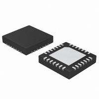
ATA5278-PKQI Atmel, ATA5278-PKQI Datasheet - Page 8

ATA5278-PKQI
Manufacturer Part Number
ATA5278-PKQI
Description
IC ANTENNA DVR STAND-ALONE 28QFN
Manufacturer
Atmel
Type
Stand Alone Antenna Driverr
Datasheet
1.ATA5278-PKQI.pdf
(34 pages)
Specifications of ATA5278-PKQI
Rf Type
TPM
Frequency
125kHz
Package / Case
28-VFQFN
Maximum Operating Temperature
+ 105 C
Mounting Style
SMD/SMT
Minimum Operating Temperature
- 40 C
Lead Free Status / RoHS Status
Lead free / RoHS Compliant
Features
-
Lead Free Status / Rohs Status
Lead free / RoHS Compliant
Other names
ATA5278-PKQITR
3.6
8
SPI
ATA5278
The control interface of the ATA5278 consists of an eight-bit synchronous SPI. It has a clock
input (S_CLK) which supports frequencies up to 1 MHz, a chip select line (S_CS) which enables
the interface, a serial data input (S_DI) and a serial data output (S_DO). The output pin is of a
tristate type, which will be set to high-impedance state as soon as the chip-select line is dis-
abled. The interface is in slave mode configuration. This means that an SPI master (e.g. a
microcontroller) is required for communication with the ATA5278, as the IC will neither start a
communication by itself nor is it able to provide the serial clock signal.
internal structure.
Figure 3-6.
Once enabled by the chip-select line, the data at the S_DI pin is shifted into the input register
with every rising edge of the input clock signal. At the pin S_DO, the actual data of the LSB of
the output register is available. The output register is shifted on every falling edge of the input
clock signal. Two timing schemes for SPI data communication are supported, which are shown
in
Figure 3-7 on page
S_CLK
S_DO
S_CS
S_Di
SPI Structure
9.
tri
MSB
MSB
6
6
Control logic/internal data bus
5
5
Internal data bus
Output register
Input register
8
4
4
8
3
3
2
2
1
1
Figure 3-6
LSB
LSB
4832D–RKE–12/07
sketches the


