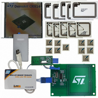
DEMOKITCRX14 STMicroelectronics, DEMOKITCRX14 Datasheet - Page 7
DEMOKITCRX14
Manufacturer Part Number
DEMOKITCRX14
Description
RFID EVALUATION KIT ISO14443-B
Manufacturer
STMicroelectronics
Type
Development kitr
Specifications of DEMOKITCRX14
Contents
CD-ROM, CRX14 Board, USB Transceiver, Samples and Documentation
Processor To Be Evaluated
CRX14
Interface Type
I2C
Operating Supply Voltage
5 V
For Use With/related Products
CRX14
Lead Free Status / RoHS Status
Contains lead / RoHS non-compliant
Other names
497-3704
Available stocks
Company
Part Number
Manufacturer
Quantity
Price
Company:

Part Number:
DEMOKITCRX14
Manufacturer:
HITACHI
Quantity:
340


SIGNAL DESCRIPTION
See
signals connected to this device.
Oscillator (OSC1, OSC2). The OSC1 and OSC2
pins are internally connected to the on-chip oscil-
lator circuit. The OSC1 pin is the input pin, the
OSC2 is the output pin. For correct operation of
the CRX14, it is required to connect a 13.56MHz
quartz crystal across OSC1 and OSC2. If an exter-
nal clock is used, it must be connected to OSC1
and OSC2 must be left open.
Antenna Output Driver (RF
Output Driver pin, RF
ed 13.56MHz signal on the antenna. Care must be
taken as it will not withstand a short-circuit.
RF
ry as shown in
must be connected across the RF
GND.
Antenna Input Filter (RF
filter of the CRX14, RF
the external antenna through an adapter circuit, as
shown in
The input filter demodulates the signal generated
on the antenna by the load variation of the PICC.
The resulting signal is then decoded by the
847kHz BPSK decoder.
Transmitter Reference Voltage (V
Transmitter Reference Voltage input, V
vides a reference voltage used by the output driver
for ASK modulation.
The Transmitter Reference Voltage input should
be connected to an external capacitor, as shown in
Figure 5.
Serial Clock (SCL). The SCL input pin is used to
strobe all I²C data in and out of the CRX14. In ap-
plications where this line is used by slave devices
to synchronize the bus to a slower clock, the mas-
ter must have an open drain output, and a pull-up
OUT
Figure
has to be connected to the antenna circuit-
Figure 5.
2., and
Figure 5.
Table
OUT
IN
The LRC antenna circuitry
, has to be connected to
1., for an overview of the
, generates the modulat-
IN
). The antenna input
OUT
). The
REF
OUT
). The
REF
Antenna
pin and
, pro-
resistor must be connected from the Serial Clock
(SCL) to V
of the pull-up resistor can be calculated).
In most applications, though, this method of syn-
chronization is not employed, and so the pull-up
resistor is not necessary, provided that the master
has a push-pull (rather than open drain) output.
Serial Data (SDA). The SDA signal is bi-direc-
tional. It is used to transfer I²C data in and out of
the CRX14. It is an open drain output that may be
wire-OR’ed with other open drain or open collector
signals on the bus. A pull-up resistor must be con-
nected from Serial data (SDA) to V
indicates how the value of the pull-up resistor can
be calculated).
Chip Enable (E0, E1, E2). The Chip Enable in-
puts E0, E1, E2 are used to set and reset the value
on the three least significant bits (b3, b2, b1) of the
7-bit I²C Device Select Code. They are used for
hardwired addressing, allowing up to eight CRX14
devices to be addressed on the same I²C bus.
These inputs may be driven dynamically or tied to
V
(note that the V
CMOS compatible, not TTL compatible).
When left open, E0, E1 and E2 are internally read
at the logic level 0 due to the internal pull-down re-
sistors connected to each inputs.
Power Supply (V
supplied to the CRX14 using the V
GND_RF pins.
V
er (+5V) for all CRX14 operations.
The GND and GND_RF pins are ground connec-
tions. They must be connected together.
Decoupling capacitors should be connected be-
tween the V
Ground pin and the GND_REF Ground pin to filter
the power line, as shown in
CC
CC
is the Power Supply pin that supplies the pow-
or GND to establish the Device Select Code
CC
. (
CC
IL
Figure 6.
Supply Voltage pin, the GND
and V
CC
, GND, GND_RF). Power is
IH
indicates how the value
levels for the inputs are
Figure 5.
CC
CC
.
, GND and
(Figure 6.
CRX14
7/40
Related parts for DEMOKITCRX14
Image
Part Number
Description
Manufacturer
Datasheet
Request
R

Part Number:
Description:
DEMO KIT M24LR-64-R
Manufacturer:
STMicroelectronics
Datasheet:

Part Number:
Description:
STMicroelectronics [RIPPLE-CARRY BINARY COUNTER/DIVIDERS]
Manufacturer:
STMicroelectronics
Datasheet:
Part Number:
Description:
STMicroelectronics [LIQUID-CRYSTAL DISPLAY DRIVERS]
Manufacturer:
STMicroelectronics
Datasheet:

Part Number:
Description:
BOARD EVAL FOR MEMS SENSORS
Manufacturer:
STMicroelectronics
Datasheet:
Part Number:
Description:
NPN TRANSISTOR POWER MODULE
Manufacturer:
STMicroelectronics
Datasheet:
Part Number:
Description:
TURBOSWITCH ULTRA-FAST HIGH VOLTAGE DIODE
Manufacturer:
STMicroelectronics
Datasheet:
Part Number:
Description:
Manufacturer:
STMicroelectronics
Datasheet:
Part Number:
Description:
DIODE / SCR MODULE
Manufacturer:
STMicroelectronics
Datasheet:
Part Number:
Description:
DIODE / SCR MODULE
Manufacturer:
STMicroelectronics
Datasheet:
Part Number:
Description:
Search -----> STE16N100
Manufacturer:
STMicroelectronics
Datasheet:
Part Number:
Description:
Search ---> STE53NA50
Manufacturer:
STMicroelectronics
Datasheet:
Part Number:
Description:
NPN Transistor Power Module
Manufacturer:
STMicroelectronics
Datasheet: