DEMOKITCRX14 STMicroelectronics, DEMOKITCRX14 Datasheet - Page 10
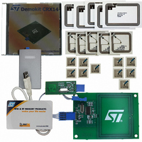
DEMOKITCRX14
Manufacturer Part Number
DEMOKITCRX14
Description
RFID EVALUATION KIT ISO14443-B
Manufacturer
STMicroelectronics
Type
Development kitr
Specifications of DEMOKITCRX14
Contents
CD-ROM, CRX14 Board, USB Transceiver, Samples and Documentation
Processor To Be Evaluated
CRX14
Interface Type
I2C
Operating Supply Voltage
5 V
For Use With/related Products
CRX14
Lead Free Status / RoHS Status
Contains lead / RoHS non-compliant
Other names
497-3704
Available stocks
Company
Part Number
Manufacturer
Quantity
Price
Company:

Part Number:
DEMOKITCRX14
Manufacturer:
HITACHI
Quantity:
340


CRX14
Input/Output Frame Register (01h)
The Input/Output Frame Register is a 36-Byte
buffer that is accessed serially from Byte 0 through
to Byte 35 (see
dress 01h.
The Input/Output Frame Register is the buffer in
which the CRX14 stores the data Bytes of the re-
quest frame to be sent to the PICC. It automatical-
ly stores the data Bytes of the answer frame
received from the PICC. The first Byte (Byte 0) of
the Input/Output Frame Register is used to store
the frame length for both transmission and recep-
tion.
When accessed in I²C Write mode , the register
stores the request frame Bytes that are to be
transmitted to the PICC. Byte 0 must be set with
the request frame length (in Bytes) and the frame
is stored from Byte 1 onwards. At the end of the
transmission, the 16-bit CRC is automatically add-
ed. After the transmission, the CRX14 wait for the
PICC to send back an answer frame. When cor-
rectly decoded, the PICC answer frame Bytes are
stored in the Input/Output Frame Register from
Table 4. Input/Output Frame Register Description
Authenticate Register (02h)
The Authenticate Register is used to trigger the
complete authentication exchange between the
CRX14 and the secured ST short range memory.
It is located at the I²C address 02h.
The Authentication system is based on a propri-
etary challenge/response mechanism that allows
the application software to authenticate a secured
ST short range memory of the SRXxxx family. A
reader designed with the CRX14 can check the
authenticity of a memory device and protect the
application system against silicon copies or emu-
lators.
A complete description of the Authentication sys-
tem is available under Non Disclosure Agreement
(NDA) with STMicroelectronics. For more details
about this CRX14 function, please contact the
nearest STMicroelectronics sales office.
Slot Marker Register (03h)
The slot Marker Register is located at the I²C ad-
dress 03h. It is used to trigger an automated anti-
10/40
Frame Length
00h No Byte transmitted
FFh CRC Error
xxh Number of transmitted Bytes
Byte 0
Table
First data Byte
4.). It is located at the I²C ad-
Byte 1
<------------- Request and Answer Frame Bytes exchanged on the RF ------------->
Second data Byte
Byte 2
Byte 1 onwards. Byte 0 stores the number of Bytes
received from the PICC.
When accessed in I²C Read mode, the Input/Out-
put Register sends back the last PICC answer
frame Bytes, if any, with Byte 0 transmitted first.
The 16-bit CRC is not stored, and it is not sent
back on the I²C bus.
The Input/Output Frame Register is set to all 00h
between transmission and reception. If there is no
answer from the PICC, Byte 0 is set to 00h. In the
case of a CRC error, Byte 0 is set to FFh, and the
data Bytes are discarded and not appended in the
register.
The CRX14 Input/Output Frame Register is so de-
signed as to generate all the ST short range mem-
ory command frames. It can also generate all
standardized ISO14443 type-B command frames
like REQB, SLOT-MARKER, ATTRIB, HALT, and
get all the answers like ATQB, or answer to AT-
TRIB. All ISO14443 type-B compliant PICCs can
be accessed by the CRX14 provided that their
data frame exchange is not longer than 35 Bytes
in both request and answer.
collision sequence between the CRX14 and any
ST short range memory present in the electromag-
netic field. With one I²C access, the CRX14
launches a complete stream of commands starting
from
SLOT_MARKER(2) up to SLOT_MARKER(15),
and stores all the identified Chip_IDs into the In-
put/Output Frame Register (I²C address 01h).
This automated anti-collision sequence simplifies
the host software development and reduces the
time needed to interrogate the 16 slots of the ST-
Microelectronics anti-collision mechanism.
When accessed in I²C Write mode, the Slot Marker
Register starts generating the sequence of anti-
collision commands. After each command, the
CRX14 wait for the ST short range memory an-
swer frame which contains the Chip_ID. The valid-
ity of the answer is checked and stored into the
corresponding Status Slot Bit (Byte 1 and Byte 2
as described in
the Status Slot Bit is set to ‘1’ and the Chip_ID is
stored into the corresponding Slot_Register. If no
answer is detected, the Status Slot Bit is set to ‘0’,
and the corresponding Slot_Register is set to 00h.
Byte 3
PCALL16(),
...
Table
Byte 34
6.). If the answer is correct,
SLOT_MARKER(1),
Last data Byte
Byte 35
Related parts for DEMOKITCRX14
Image
Part Number
Description
Manufacturer
Datasheet
Request
R

Part Number:
Description:
DEMO KIT M24LR-64-R
Manufacturer:
STMicroelectronics
Datasheet:

Part Number:
Description:
STMicroelectronics [RIPPLE-CARRY BINARY COUNTER/DIVIDERS]
Manufacturer:
STMicroelectronics
Datasheet:
Part Number:
Description:
STMicroelectronics [LIQUID-CRYSTAL DISPLAY DRIVERS]
Manufacturer:
STMicroelectronics
Datasheet:

Part Number:
Description:
BOARD EVAL FOR MEMS SENSORS
Manufacturer:
STMicroelectronics
Datasheet:
Part Number:
Description:
NPN TRANSISTOR POWER MODULE
Manufacturer:
STMicroelectronics
Datasheet:
Part Number:
Description:
TURBOSWITCH ULTRA-FAST HIGH VOLTAGE DIODE
Manufacturer:
STMicroelectronics
Datasheet:
Part Number:
Description:
Manufacturer:
STMicroelectronics
Datasheet:
Part Number:
Description:
DIODE / SCR MODULE
Manufacturer:
STMicroelectronics
Datasheet:
Part Number:
Description:
DIODE / SCR MODULE
Manufacturer:
STMicroelectronics
Datasheet:
Part Number:
Description:
Search -----> STE16N100
Manufacturer:
STMicroelectronics
Datasheet:
Part Number:
Description:
Search ---> STE53NA50
Manufacturer:
STMicroelectronics
Datasheet:
Part Number:
Description:
NPN Transistor Power Module
Manufacturer:
STMicroelectronics
Datasheet: