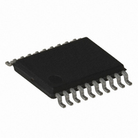
AT86RF401U-XI Atmel, AT86RF401U-XI Datasheet - Page 27

AT86RF401U-XI
Manufacturer Part Number
AT86RF401U-XI
Description
IC MICRO TX RF W/AVR 20-TSSOP
Manufacturer
Atmel
Datasheet
1.AT86RF401U-6GS.pdf
(52 pages)
Specifications of AT86RF401U-XI
Frequency
264MHz ~ 456MHz
Applications
Garage Opener, RKE, Telemetry
Modulation Or Protocol
ASK, OOK
Data Rate - Maximum
10 kbps
Power - Output
6dBm
Current - Transmitting
23.2mA
Data Interface
PCB, Surface Mount
Antenna Connector
PCB, Surface Mount
Memory Size
2KB Flash, 128 Byte EEPROM, 128Byte SRAM
Voltage - Supply
2 V ~ 5 V
Operating Temperature
-40°C ~ 85°C
Package / Case
20-TSSOP
Lead Free Status / RoHS Status
Contains lead / RoHS non-compliant
Features
-
Other names
AT86RF401U
1424F–RKE–12/03
The internal data SRAM access is performed in two System Clock cycles as described
in Figure 24.
Figure 24. On-chip Data SRAM Access Cycles
All I/Os and peripherals are placed in the I/O space. The I/O locations are accessed by
the IN and OUT instructions, transferring data between the 32 general-purpose working
registers and the I/O space. I/O registers within the address range $00–$1F are directly
bit-accessible using the SBI and CBI instructions. In these registers, the value of single
bits can be checked by using the SBIS and SBIC instructions. Refer to Table 10,
“Instruction Set Manual,” on page 44 for more details. When using the I/O specific com-
mands IN and OUT, the I/O addresses $00–$3F must be used. When addressing I/O
registers as SRAM, $20 must be added to these addresses.
For compatibility with future devices, reserved bits should be written to “0” if accessed.
Reserved I/O memory addresses should never be written.
Some of the status flags are cleared by writing a logical “1” to them. Note that the CBI
and SBI instructions will operate on all bits in the I/O register, writing a “1” back into any
flag read as set, thus clearing the flag. The CBI and SBI instructions work with registers
$00 to $1F only.
The I/O and peripherals control registers are explained in the following sections.
System Clock Ø
Address
Write
Read
Data
Data
Prev. Address
T1
Address
T2
T3
AT86RF401
T4
27


