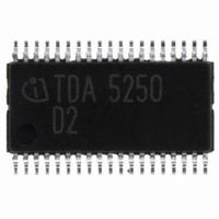
TDA5250 Infineon Technologies, TDA5250 Datasheet - Page 67

TDA5250
Manufacturer Part Number
TDA5250
Description
TX/RX ASK/FSK 868-870MHZ 38TSSOP
Manufacturer
Infineon Technologies
Type
Transceiverr
Specifications of TDA5250
Package / Case
38-TSSOP
Frequency
868MHz
Data Rate - Maximum
64kbps
Modulation Or Protocol
ASK, FSK
Applications
RKE, Remote Control Systems
Power - Output
9dBm
Sensitivity
-109dBm
Voltage - Supply
2.1 V ~ 5.5 V
Current - Receiving
9mA
Current - Transmitting
12mA
Data Interface
PCB, Surface Mount
Antenna Connector
PCB, Surface Mount
Operating Temperature
-40°C ~ 85°C
Operating Frequency
870 MHz
Operating Supply Voltage
2.5 V, 3.3 V, 5 V
Maximum Operating Temperature
+ 85 C
Minimum Operating Temperature
- 40 C
Mounting Style
SMD/SMT
Operating Temperature (min)
-40C
Operating Temperature (max)
85C
Operating Temperature Classification
Industrial
Product Depth (mm)
4.4mm
Product Length (mm)
9.7mm
Operating Supply Voltage (min)
2.1V
Operating Supply Voltage (max)
5.5V
Lead Free Status / RoHS Status
Lead free / RoHS Compliant
Memory Size
-
Lead Free Status / Rohs Status
Compliant
Other names
SP000012956
TDA5250
TDA5250INTR
TDA5250XT
TDA5250XT
TDA5250
TDA5250INTR
TDA5250XT
TDA5250XT
Available stocks
Company
Part Number
Manufacturer
Quantity
Price
Company:
Part Number:
TDA5250
Manufacturer:
Infineon Technologies
Quantity:
135
Company:
Part Number:
TDA5250D2
Manufacturer:
INFINEON
Quantity:
300
Part Number:
TDA5250D2
Manufacturer:
INFINEON/英飞凌
Quantity:
20 000
Component calculation: (rule of thumb)
3.6.3
The TDA5250 data output can be digital (pin 28) or in analog form by using the peak detector output
and changing some settings.
To get an analog data output the slicer must be set to lowpass mode (Reg. 0, D15 = LP = 0) and
the peak detector capacitor at pin 12 or 13 has to be changed to a resistor of about 47kOhm.
Figure 3-28
3.6.4
For a safe and fast threshold value generation the peak detector is turned on by the sequencer
circuit (see Section 2.4.18) only after the entire receiving path is active.
In the off state the output of the positive peak detector is tied down to GND and the output of the
negative peak detector is pulled up to VCC.
Data Sheet
C
C
p
n
≥
≥
2
2
100k
100k
⋅
⋅
T
T
L2
L1
Ω
Ω
Peak Detector - Analog output signal
Peak Detector – Power Down Mode
Peak Detector as analog Buffer (v=1)
T
T
L1
L2
– longest period of no signal change (LOW signal)
– longest period of no signal change (HIGH signal)
67
TDA5250 D2
Version 1.7
[3 – 35]
[3 – 34]
Application
2007-02-26
PkD_analog.wmf


