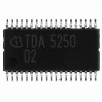
TDA5250 Infineon Technologies, TDA5250 Datasheet - Page 35

TDA5250
Manufacturer Part Number
TDA5250
Description
TX/RX ASK/FSK 868-870MHZ 38TSSOP
Manufacturer
Infineon Technologies
Type
Transceiverr
Specifications of TDA5250
Package / Case
38-TSSOP
Frequency
868MHz
Data Rate - Maximum
64kbps
Modulation Or Protocol
ASK, FSK
Applications
RKE, Remote Control Systems
Power - Output
9dBm
Sensitivity
-109dBm
Voltage - Supply
2.1 V ~ 5.5 V
Current - Receiving
9mA
Current - Transmitting
12mA
Data Interface
PCB, Surface Mount
Antenna Connector
PCB, Surface Mount
Operating Temperature
-40°C ~ 85°C
Operating Frequency
870 MHz
Operating Supply Voltage
2.5 V, 3.3 V, 5 V
Maximum Operating Temperature
+ 85 C
Minimum Operating Temperature
- 40 C
Mounting Style
SMD/SMT
Operating Temperature (min)
-40C
Operating Temperature (max)
85C
Operating Temperature Classification
Industrial
Product Depth (mm)
4.4mm
Product Length (mm)
9.7mm
Operating Supply Voltage (min)
2.1V
Operating Supply Voltage (max)
5.5V
Lead Free Status / RoHS Status
Lead free / RoHS Compliant
Memory Size
-
Lead Free Status / Rohs Status
Compliant
Other names
SP000012956
TDA5250
TDA5250INTR
TDA5250XT
TDA5250XT
TDA5250
TDA5250INTR
TDA5250XT
TDA5250XT
Available stocks
Company
Part Number
Manufacturer
Quantity
Price
Company:
Part Number:
TDA5250
Manufacturer:
Infineon Technologies
Quantity:
135
Company:
Part Number:
TDA5250D2
Manufacturer:
INFINEON
Quantity:
300
Part Number:
TDA5250D2
Manufacturer:
INFINEON/英飞凌
Quantity:
20 000
With default settings the clock generating units are disabled during PD, therefore no clock is
available at the clock output pin. It is possible to offer a clock signal at the clock output pin every
time (also during PD) if the CLK_EN Bit in the CONFIG register is set to HIGH.
Figure 2-15
Note: The time values are typical values
Figure 2-16
*
Note: The time values are typical values
Data Sheet
DC OFFSET COMPENSATION
State is either „I“ or „O“ depending on time of setting into powerdown.
DC OFFSET COMPENSATION
PEAK DETECTOR EN
DATADETECTION EN
POWER AMP EN
PEAK DETECTOR EN
DATADETECTION EN
POWER AMP EN
XTAL EN
STATUS
0.5ms
t
XTAL EN
CLKSU
STATUS
0.5ms
1
t
1st start or reset in PD mode
CLKSU
st
start or reset in active mode
RESET
or 1
PWDDD = low
TX activ or RX activ
RESET
or 1
PWDDD = high
st
POWER ON
st
POWER ON
CLOCK FOR EXTERNAL µP
t
SYSSU
CLOCK FOR EXTERNAL µP
8ms
1.1ms
t
TXSU
PD
if RX
if RX
if RX
if TX
t
2.2ms
t
2.6ms
RXSU
DDSU
PWDDD = low
t
0.5ms
CLKSU
35
PD
*
TX activ or RX activ
t
SYSSU
8ms
1.1ms
t
TX activ
TXSU
t
1.1ms
TXSU
if RX
t
0.5ms
CLKSU
PD
*
if RX
if RX
if TX
t
2.2ms
t
2.6ms
RXSU
DDSU
RX activ
0.5ms
Functional Description
t
CLKSU
PD
*
t
2.2ms
t
2.6ms
RXSU
DDSU
TX activ
Sequenzer_Timing_pupstart.wmf
TX activ
t
1.1ms
Sequenzer_Timing_pdstart.wmf
TXSU
t
1.1ms
TXSU
TDA5250 D2
Version 1.7
RX activ
RX activ
2007-02-26
t
2.2ms
t
2.6ms
t
2.2ms
t
2.6ms
RXSU
DDSU
RXSU
DDSU


