RN-800S-CB Roving Networks Inc, RN-800S-CB Datasheet - Page 9
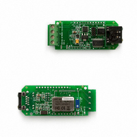
RN-800S-CB
Manufacturer Part Number
RN-800S-CB
Description
MODULE A/D BLUETOOTH BLUESENTRY
Manufacturer
Roving Networks Inc
Specifications of RN-800S-CB
Frequency
2.4GHz
Modulation Or Protocol
Bluetooth v2.0, Class 1
Applications
Sensor Interface - Ready To Go Module
Power - Output
15dBm
Voltage - Supply
6 V ~ 12 V
Data Interface
PCB, Surface Mount
Antenna Connector
PCB, Surface Mount
Package / Case
Module
Antenna
Chip Antenna
Board Size
1.6 in x 3 in x 0.9 in
Lead Free Status / RoHS Status
Lead free / RoHS Compliant
Operating Temperature
-
Sensitivity
-
Memory Size
-
Data Rate - Maximum
-
Current - Transmitting
-
Current - Receiving
-
Lead Free Status / Rohs Status
Lead free / RoHS Compliant
Other names
740-1011


FIGURE 1. Basic Operation of the ADS8344.
ADS8344
TABLE I. Single-Ended Channel Selection (SGL/DIF HIGH).
THEORY OF OPERATION
The ADS8344 is a classic Successive Approximation
Register (SAR) Analog-to-Digital (A/D) converter. The ar-
chitecture is based on capacitive redistribution which inher-
ently includes a sample/hold function. The converter is
fabricated on a 0.6 s CMOS process.
The basic operation of the ADS8344 is shown in Figure 1.
The device requires an external reference and an external
clock. It operates from a single supply of 2.7V to 5.25V. The
external reference can be any voltage between 500mV and
+V
input range of the converter. The average reference input
current depends on the conversion rate of the ADS8344.
The analog input to the converter is differential and is
provided via an eight-channel multiplexer. The input can be
provided in reference to a voltage on the COM pin (which
is generally ground) or differentially by using four of the
eight input channels (CH0 - CH7). The particular configura-
tion is selectable via the digital interface.
A2
0
1
0
1
0
1
0
1
SBAS139B
CC
. The value of the reference voltage directly sets the
A1
0
0
0
0
1
1
1
1
A0
0
0
1
1
0
0
1
1
CH0 CH1 CH2 CH3 CH4 CH5 CH6 CH7 COM
+IN
Single-ended
or differential
analog inputs
+IN
+IN
+IN
+IN
+IN
+IN
10
1
2
3
4
5
6
7
8
9
+IN
CH0
CH1
CH2
CH3
CH4
CH5
CH6
CH7
COM
SHDN
ADS8344
–IN
–IN
–IN
–IN
–IN
–IN
–IN
–IN
BUSY
DCLK
+V
+V
D
GND
GND
V
OUT
CS
D
REF
CC
CC
IN
TABLE II. Differential Channel Control (SGL/DIF LOW).
ANALOG INPUT
See Figure 2 for a block diagram of the input multiplexer on
the ADS8344. The differential input of the converter is
derived from one of the eight inputs in reference to the COM
pin, or four of the eight inputs. Table I and Table II show the
relationship between the A2, A1, A0, and SGL/DIF control
bits and the configuration of the analog multiplexer. The
control bits are provided serially via the D
Digital Interface section of this data sheet for more details).
When the converter enters the hold mode, the voltage
difference between the +IN and –IN inputs is captured on
the internal capacitor array (see Figure 2). The voltage on
the –IN input is limited between –0.2V and 1.25V, allowing
the input to reject small signals which are common to both
the +IN and –IN input. The +IN input has a range of –0.2V
to +V
The input current on the analog inputs depends on the conver-
sion rate of the device. During the sample period, the source
must charge the internal sampling capacitor (typically 25pF).
After the capacitor has been fully charged, there is no further
input current. The rate of charge transfer from the analog
source to the converter is a function of conversion rate.
20
19
18
17
16
15
14
13
12
11
A2
0
0
0
0
1
1
1
1
A1
CC
0
0
1
1
0
0
1
1
+2.7V to +5V
+ 0.2V.
A0
0
1
0
1
0
1
0
1
CH0
+IN
–IN
1 F to 10 F
0.1 F
Serial/Conversion Clock
Chip Select
Serial Data In
Serial Data Out
CH1
–IN
+IN
CH2
+IN
–IN
1 F to 10 F
CH3
–IN
+IN
CH4
+IN
–IN
CH5
–IN
+IN
IN
pin (see the
CH6
+IN
–IN
CH7
–IN
+IN
9
Related parts for RN-800S-CB
Image
Part Number
Description
Manufacturer
Datasheet
Request
R

Part Number:
Description:
MODULE BLUETOOTH SENSOR SMA
Manufacturer:
Roving Networks Inc
Datasheet:

Part Number:
Description:
Spacer
Manufacturer:
SPC TECHNOLOGY
Datasheet:

Part Number:
Description:
Spacer
Manufacturer:
SPC TECHNOLOGY
Datasheet:

Part Number:
Description:
Spacer
Manufacturer:
SPC TECHNOLOGY
Datasheet:

Part Number:
Description:
Spacer
Manufacturer:
SPC TECHNOLOGY
Datasheet:

Part Number:
Description:
Spacer
Manufacturer:
SPC TECHNOLOGY
Datasheet:

Part Number:
Description:
RES MF 1/8W 10.8K OHM 1% AXIAL
Manufacturer:
Stackpole Electronics Inc
Datasheet:
Part Number:
Description:
RES MF 1/8W 9.9K OHM 1% AXIAL
Manufacturer:
Stackpole Electronics Inc
Datasheet:

Part Number:
Description:
CONV DC/DC 1.25W 05VIN 09VOUT
Manufacturer:
Recom Power Inc
Datasheet:
Part Number:
Description:
CONV DC/DC 1.25W 05VIN 12VOUT
Manufacturer:
Recom Power Inc
Datasheet:
Part Number:
Description:
CONV DC/DC 1.25W 09VIN 15VOUT
Manufacturer:
Recom Power Inc
Datasheet:
Part Number:
Description:
CONV DC/DC 1.25W 09VIN 24VOUT
Manufacturer:
Recom Power Inc
Datasheet:

Part Number:
Description:
MODULE SOCKET BLUETOOTH CLASS1
Manufacturer:
Roving Networks Inc
Datasheet:

Part Number:
Description:
MODULE BLUETOOTH V2.1+EDR
Manufacturer:
Roving Networks Inc
Datasheet: