RN-800S-CB Roving Networks Inc, RN-800S-CB Datasheet - Page 10
RN-800S-CB
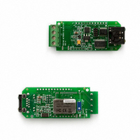
Manufacturer Part Number
RN-800S-CB
Description
MODULE A/D BLUETOOTH BLUESENTRY
Manufacturer
Roving Networks Inc
Specifications of RN-800S-CB
Frequency
2.4GHz
Modulation Or Protocol
Bluetooth v2.0, Class 1
Applications
Sensor Interface - Ready To Go Module
Power - Output
15dBm
Voltage - Supply
6 V ~ 12 V
Data Interface
PCB, Surface Mount
Antenna Connector
PCB, Surface Mount
Package / Case
Module
Antenna
Chip Antenna
Board Size
1.6 in x 3 in x 0.9 in
Lead Free Status / RoHS Status
Lead free / RoHS Compliant
Operating Temperature
-
Sensitivity
-
Memory Size
-
Data Rate - Maximum
-
Current - Transmitting
-
Current - Receiving
-
Lead Free Status / Rohs Status
Lead free / RoHS Compliant
Other names
740-1011


FIGURE 3. Conversion Timing, 24-Clocks per Conversion, 8-Bit Bus Interface. No DCLK delay required with dedicated
FIGURE 2. Simplified Diagram of the Analog Input.
REFERENCE INPUT
The external reference sets the analog input range. The
ADS8344 will operate with a reference in the range of
100mV to +V
difference between the +IN input and the –IN input, as
shown in Figure 2. For example, in the single-ended mode,
a 1.25V reference with the COM pin grounded, the selected
input channel (CH0 - CH7) will properly digitize a signal in
the range of 0V to 1.25V. If the COM pin is connected to
0.5V, the input range on the selected channel is 0.5V to
1.75V.
There are several critical items concerning the reference
input and its wide-voltage range. As the reference voltage is
reduced, the analog voltage weight of each digital output
code is also reduced. This is often referred to as the LSB
10
BUSY
DCLK
D
COM
NOTE: (1) See Truth Tables, Table I
and Table II for address coding.
OUT
D
CS
CH0
CH4
CH1
CH2
CH3
CH5
CH6
CH7
IN
(START)
serial port.
S
1
CC
Idle
A2
. Keep in mind that the analog input is the
A1
A0
SGL/
DIF PD1 PD0
(shown 00o
Acquire
t
ACQ
A2-A0
8
(shown HIGH)
B
SGL/DIF
)
(1)
1
(MSB)
15
14
+IN
–IN
13
Converter
12
11
10
Conversion
9
8
8
1
(Least Significant Bit) size and is equal to the reference
voltage divided by 65536. Any offset or gain error inherent
in the A/D converter will appear to increase, in terms of LSB
size, as the reference voltage is reduced. For example, if the
offset of a given converter is 2LSBs with a 2.5V reference,
then it will typically be 10LSBs with a 0.5V reference. In
each case, the actual offset of the device is the same,
76.3 V.
Likewise, the noise or uncertainty of the digitized output
will increase with lower LSB size. With a reference voltage
of 500mV, the LSB size is 7.6 V. This level is below the
internal noise of the device. As a result, the digital output
code will not be stable and will vary around a mean value by
a number of LSBs. The distribution of output codes will be
gaussian and the noise can be reduced by simply averaging
consecutive conversion results or applying a digital filter.
With a lower reference voltage, care should be taken to
provide a clean layout including adequate bypassing, a clean
(low-noise, low-ripple) power supply, a low-noise reference,
and a low-noise input signal. Because the LSB size is lower,
the converter will also be more sensitive to nearby digital
signals and electromagnetic interference.
The voltage into the V
drives the Capacitor Digital-to-Analog Converter (CDAC)
portion of the ADS8344. Typically, the input current is
13 A with a 2.5V reference. This value will vary by
microamps depending on the result of the conversion. The
reference current diminishes directly with both conversion
rate and reference voltage. As the current from the reference
is drawn on each bit decision, clocking the converter more
quickly during a given conversion period will not reduce
overall current drain from the reference.
DIGITAL INTERFACE
The ADS8344 has a four-wire serial interface compatible
with several microprocessor families (note that the digital
inputs are over-voltage tolerant up to +5.5V, regardless of
+V
digital interface.
Most microprocessors communicate using 8-bit transfers;
the ADS8344 can complete a conversion with three such
transfers, for a total of 24 clock cycles on the DCLK input,
provided the timing is as shown in Figure 3.
7
CC
6
). Figure 3 shows the typical operation of the ADS8344
5
4
3
2
1
8
REF
(START)
(LSB)
0
S
1
input is not buffered and directly
A2
Idle
A1
A0
Zero Filled...
SGL/
DIF PD1 PD0
Acquire
ADS8344
8
SBAS139B
1
Conversion
(MSB)
15
14
Related parts for RN-800S-CB
Image
Part Number
Description
Manufacturer
Datasheet
Request
R

Part Number:
Description:
MODULE BLUETOOTH SENSOR SMA
Manufacturer:
Roving Networks Inc
Datasheet:

Part Number:
Description:
Spacer
Manufacturer:
SPC TECHNOLOGY
Datasheet:

Part Number:
Description:
Spacer
Manufacturer:
SPC TECHNOLOGY
Datasheet:

Part Number:
Description:
Spacer
Manufacturer:
SPC TECHNOLOGY
Datasheet:

Part Number:
Description:
Spacer
Manufacturer:
SPC TECHNOLOGY
Datasheet:

Part Number:
Description:
Spacer
Manufacturer:
SPC TECHNOLOGY
Datasheet:

Part Number:
Description:
RES MF 1/8W 10.8K OHM 1% AXIAL
Manufacturer:
Stackpole Electronics Inc
Datasheet:
Part Number:
Description:
RES MF 1/8W 9.9K OHM 1% AXIAL
Manufacturer:
Stackpole Electronics Inc
Datasheet:

Part Number:
Description:
CONV DC/DC 1.25W 05VIN 09VOUT
Manufacturer:
Recom Power Inc
Datasheet:
Part Number:
Description:
CONV DC/DC 1.25W 05VIN 12VOUT
Manufacturer:
Recom Power Inc
Datasheet:
Part Number:
Description:
CONV DC/DC 1.25W 09VIN 15VOUT
Manufacturer:
Recom Power Inc
Datasheet:
Part Number:
Description:
CONV DC/DC 1.25W 09VIN 24VOUT
Manufacturer:
Recom Power Inc
Datasheet:

Part Number:
Description:
MODULE SOCKET BLUETOOTH CLASS1
Manufacturer:
Roving Networks Inc
Datasheet:

Part Number:
Description:
MODULE BLUETOOTH V2.1+EDR
Manufacturer:
Roving Networks Inc
Datasheet: