RN-800S-CB Roving Networks Inc, RN-800S-CB Datasheet - Page 11
RN-800S-CB
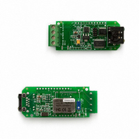
Manufacturer Part Number
RN-800S-CB
Description
MODULE A/D BLUETOOTH BLUESENTRY
Manufacturer
Roving Networks Inc
Specifications of RN-800S-CB
Frequency
2.4GHz
Modulation Or Protocol
Bluetooth v2.0, Class 1
Applications
Sensor Interface - Ready To Go Module
Power - Output
15dBm
Voltage - Supply
6 V ~ 12 V
Data Interface
PCB, Surface Mount
Antenna Connector
PCB, Surface Mount
Package / Case
Module
Antenna
Chip Antenna
Board Size
1.6 in x 3 in x 0.9 in
Lead Free Status / RoHS Status
Lead free / RoHS Compliant
Operating Temperature
-
Sensitivity
-
Memory Size
-
Data Rate - Maximum
-
Current - Transmitting
-
Current - Receiving
-
Lead Free Status / Rohs Status
Lead free / RoHS Compliant
Other names
740-1011


ADS8344
The first eight clock cycles are used to provide the control
byte via the D
information about the following conversion to set the input
multiplexer appropriately, it enters the acquisition (sample)
mode. After four more clock cycles, the control byte is
complete and the converter enters the conversion mode. At
this point, the input sample/hold goes into the Hold mode.
The next sixteen clock cycles accomplish the actual A/D
conversion.
Control Byte
See Figure 3 for placement and order of the control bits
within the control byte. Tables III and IV give detailed
information about these bits. The first bit, the “S” bit, must
always be HIGH and indicates the start of the control byte.
The ADS8344 will ignore inputs on the D
START bit is detected. The next three bits (A2-A0) select
the active input channel or channels of the input multiplexer
(see Tables I and II and Figure 2).
The SGL/DIF-bit controls the multiplexer input mode: ei-
ther in single-ended mode, where the selected input channel
is referenced to the COM pin, or in differential mode, where
the two selected inputs provide a differential input.
TABLE III. Order of the Control Bits in the Control Byte.
TABLE IV. Descriptions of the Control Bits within the
FIGURE 4. Detailed Timing Diagram.
(MSB)
BIT 7
BIT
7
6 - 4
2
1 - 0
SBAS139B
S
PD1 - PD0
SGL/DIF
BIT 6
A2 - A0
NAME
A2
S
Control Byte.
DCLK
BUSY
D
BIT 5
IN
OUT
D
CS
A1
DESCRIPTION
Start Bit. Control byte starts with first HIGH bit on
D
Channel Select Bits. Along with the SGL/DIF bit,
these bits control the setting of the multiplexer input,
as detailed in Tables I and II.
Single-Ended/Differential Select Bit. Along with bits
A2 - A0, this bit controls the setting of the multiplexer
input, as detailed in Tables I and II.
Power-Down Mode Select Bits. See Table V for
details.
IN
IN
pin. When the converter has enough
.
BIT 4
A0
t
CSS
t
t
DV
BDV
BIT 3
—
t
DS
SGL/DIF
t
BIT 2
CH
IN
BIT 1
PD1
pin until the
t
DH
BIT 0
(LSB)
t
CL
PD0
PD0
t
BD
See Tables I and II and Figure 2 for more information. The
last two bits (PD1 - PD0) select the power-down mode and
Clock mode, as shown in Table V. If both PD1 and PD0 are
HIGH, the device is always powered up. If both PD1 and
PD0 are LOW, the device enters a power-down mode
between conversions. When a new conversion is initiated,
the device will resume normal operation instantly—no delay
is needed to allow the device to power up and the very first
conversion will be valid.
Clock Modes
The ADS8344 can be used with an external serial clock or an
internal clock to perform the successive-approximation con-
version. In both clock modes, the external clock shifts data in
and out of the device. Internal clock mode is selected when
PD1 is HIGH and PD0 is LOW.
If the user decides to switch from one clock mode to the other,
an extra conversion cycle will be required before the
ADS8344 can switch to the new mode. The extra cycle is
required because the PD0 and PD1 control bits need to be
written to the ADS8344 prior to the change in clock modes.
NOTE: It is recommended that the customer write to the PD1
and PD0 registers prior to the first conversion in order to
insure that the proper clock mode is selected.
External Clock Mode
In external clock mode, the external clock not only shifts data
in and out of the ADS8344, it also controls the A/D conversion
steps. BUSY will go HIGH for one clock period after the last
bit of the control byte is shifted in. Successive-approximation
bit decisions are made and appear at D
16 S
BUSY timing in external clock mode.
TABLE V. Power-Down Selection.
t
BD
PD1
0
1
0
1
DCLK
falling edges (see Figure 3). Figure 4 shows the
15
PD0
0
0
1
1
t
D0
14
conversion is finished, the converter enters a
low-power mode. At the start of the next conver-
sion, the device instantly powers up to full power.
There is no need for additional delays to assure full
operation and the very first conversion is valid.
ways powered.
DESCRIPTION
Power-down between conversions. When each
Internal clock mode.
Reserved for future use.
No power-down between conversions, device al-
t
t
CSH
BTR
t
TR
OUT
on each of the next
11
Related parts for RN-800S-CB
Image
Part Number
Description
Manufacturer
Datasheet
Request
R

Part Number:
Description:
MODULE BLUETOOTH SENSOR SMA
Manufacturer:
Roving Networks Inc
Datasheet:

Part Number:
Description:
Spacer
Manufacturer:
SPC TECHNOLOGY
Datasheet:

Part Number:
Description:
Spacer
Manufacturer:
SPC TECHNOLOGY
Datasheet:

Part Number:
Description:
Spacer
Manufacturer:
SPC TECHNOLOGY
Datasheet:

Part Number:
Description:
Spacer
Manufacturer:
SPC TECHNOLOGY
Datasheet:

Part Number:
Description:
Spacer
Manufacturer:
SPC TECHNOLOGY
Datasheet:

Part Number:
Description:
RES MF 1/8W 10.8K OHM 1% AXIAL
Manufacturer:
Stackpole Electronics Inc
Datasheet:
Part Number:
Description:
RES MF 1/8W 9.9K OHM 1% AXIAL
Manufacturer:
Stackpole Electronics Inc
Datasheet:

Part Number:
Description:
CONV DC/DC 1.25W 05VIN 09VOUT
Manufacturer:
Recom Power Inc
Datasheet:
Part Number:
Description:
CONV DC/DC 1.25W 05VIN 12VOUT
Manufacturer:
Recom Power Inc
Datasheet:
Part Number:
Description:
CONV DC/DC 1.25W 09VIN 15VOUT
Manufacturer:
Recom Power Inc
Datasheet:
Part Number:
Description:
CONV DC/DC 1.25W 09VIN 24VOUT
Manufacturer:
Recom Power Inc
Datasheet:

Part Number:
Description:
MODULE SOCKET BLUETOOTH CLASS1
Manufacturer:
Roving Networks Inc
Datasheet:

Part Number:
Description:
MODULE BLUETOOTH V2.1+EDR
Manufacturer:
Roving Networks Inc
Datasheet: