RN-800S-CB Roving Networks Inc, RN-800S-CB Datasheet - Page 13
RN-800S-CB
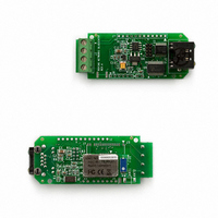
Manufacturer Part Number
RN-800S-CB
Description
MODULE A/D BLUETOOTH BLUESENTRY
Manufacturer
Roving Networks Inc
Specifications of RN-800S-CB
Frequency
2.4GHz
Modulation Or Protocol
Bluetooth v2.0, Class 1
Applications
Sensor Interface - Ready To Go Module
Power - Output
15dBm
Voltage - Supply
6 V ~ 12 V
Data Interface
PCB, Surface Mount
Antenna Connector
PCB, Surface Mount
Package / Case
Module
Antenna
Chip Antenna
Board Size
1.6 in x 3 in x 0.9 in
Lead Free Status / RoHS Status
Lead free / RoHS Compliant
Operating Temperature
-
Sensitivity
-
Memory Size
-
Data Rate - Maximum
-
Current - Transmitting
-
Current - Receiving
-
Lead Free Status / Rohs Status
Lead free / RoHS Compliant
Other names
740-1011


ADS8344
TABLE VII. Timing Specifications (+V
Data Format
The ADS8344 output data is in straight binary format, as
shown in Figure 7. This figure shows the ideal output code
for the given input voltage and does not include the effects
of offset, gain, or noise.
FIGURE 7. Ideal Input Voltages and Output Codes.
POWER DISSIPATION
There are three power modes for the ADS8344: full-power
(PD1 - PD0 = 11B), auto power-down (PD1 - PD0 = 00B),
and shutdown (SHDN LOW). The effects of these modes
varies depending on how the ADS8344 is being operated.
For example, at full conversion rate and 24-clocks per
conversion, there is very little difference between
full-power mode and auto power-down; a shutdown will not
lower power dissipation.
When operating at full-speed and 24-clocks per conversion
(see Figure 3), the ADS8344 spends most of its time
acquiring or converting. There is little time for auto
power-down, assuming that this mode is active. Thus, the
difference between full-power mode and auto power-down
is negligible. If the conversion rate is decreased by simply
slowing the frequency of the DCLK input, the two modes
SYMBOL
NOTE: (1) Voltage at converter input, after multiplexer: +IN–(–IN). (See Figure 2.)
SBAS139B
t
t
t
t
t
t
ACQ
t
t
t
t
CSS
CSH
t
t
t
BDV
BTR
DH
DO
CH
DS
DV
TR
CL
BD
11...111
11...110
11...101
00...010
00...001
00...000
CS Falling to First DCLK Rising
D
DCLK Falling to BUSY Rising
CS Rising to BUSY Disabled
CS Falling to BUSY Enabled
CS Falling to D
CS Rising to D
CS Rising to DCLK Ignored
IN
DCLK Falling to D
D
IN
Valid Prior to DCLK Rising
+5.25V, T
Hold After DCLK HIGH
Acquisition Time
0V
DESCRIPTION
DCLK HIGH
DCLK LOW
FS = Full-Scale Voltage = V
OUT
OUT
A
1 LSB
OUT
Disabled
= –40 C to +85 C, C
Enabled
1 LSB = V
Input Voltage
Valid
REF
/65,536
(1)
MIN
150
150
1.7
50
10
50
0
(V)
REF
TYP
CC
FS – 1 LSB
LOAD
= +4.75V to
MAX
100
100
70
70
70
70
= 50pF).
UNITS
ns
ns
ns
ns
ns
ns
ns
ns
ns
ns
ns
ns
s
remain approximately equal. However, if the DCLK fre-
quency is kept at the maximum rate during a conversion, but
conversions are simply done less often, then the difference
between the two modes is dramatic. In the latter case, the
converter spends an increasing percentage of its time in
power-down mode (assuming the auto power-down mode is
active).
If DCLK is active and CS is LOW while the ADS8344 is in
auto power-down mode, the device will continue to dissipate
some power in the digital logic. The power can be reduced
to a minimum by keeping CS HIGH.
Operating the ADS8344 in auto power-down mode will
result in the lowest power dissipation, and there is no
conversion time “penalty” on power-up. The very first
conversion will be valid. SHDN can be used to force an
immediate power-down.
NOISE
The noise floor of the ADS8344 itself is extremely low, as
shown in Figures 8 thru 11, and is much lower than compet-
ing A/D converters. The ADS8344 was tested at both 5V
and 2.7V, and in both the internal and external clock modes.
A low-level DC input was applied to the analog-input pins
and the converter was put through 5,000 conversions. The
digital output of the A/D converter will vary in output code
due to the internal noise of the ADS8344. This is true for all
16-bit SAR-type A/D converters. Using a histogram to plot
the output codes, the distribution should appear bell-shaped
with the peak of the bell curve representing the nominal code
for the input value. The 1 , 2 , and 3 distributions will
represent the 68.3%, 95.5%, and 99.7%, respectively, of all
codes. The transition noise can be calculated by dividing the
number of codes measured by 6 and this will yield the 3
distribution, or 99.7%, of all codes. Statistically, up to 3
codes could fall outside the distribution when executing
1,000 conversions. The ADS8344, with < 3 output codes for
the 3 distribution, will yield a < 0.5LSB transition noise
at 5V operation. Remember, to achieve this low-noise per-
formance, the peak-to-peak noise of the input signal and
reference must be < 50 V.
FIGURE 8. Histogram of 5,000 Conversions of a DC Input at the
Code Transition, 5V operation external clock mode.
7FFD
0
7FFE
242
7FFF
Code
4561
8000
197
8001
0
13
Related parts for RN-800S-CB
Image
Part Number
Description
Manufacturer
Datasheet
Request
R

Part Number:
Description:
MODULE BLUETOOTH SENSOR SMA
Manufacturer:
Roving Networks Inc
Datasheet:

Part Number:
Description:
Spacer
Manufacturer:
SPC TECHNOLOGY
Datasheet:

Part Number:
Description:
Spacer
Manufacturer:
SPC TECHNOLOGY
Datasheet:

Part Number:
Description:
Spacer
Manufacturer:
SPC TECHNOLOGY
Datasheet:

Part Number:
Description:
Spacer
Manufacturer:
SPC TECHNOLOGY
Datasheet:

Part Number:
Description:
Spacer
Manufacturer:
SPC TECHNOLOGY
Datasheet:

Part Number:
Description:
RES MF 1/8W 10.8K OHM 1% AXIAL
Manufacturer:
Stackpole Electronics Inc
Datasheet:
Part Number:
Description:
RES MF 1/8W 9.9K OHM 1% AXIAL
Manufacturer:
Stackpole Electronics Inc
Datasheet:

Part Number:
Description:
CONV DC/DC 1.25W 05VIN 09VOUT
Manufacturer:
Recom Power Inc
Datasheet:
Part Number:
Description:
CONV DC/DC 1.25W 05VIN 12VOUT
Manufacturer:
Recom Power Inc
Datasheet:
Part Number:
Description:
CONV DC/DC 1.25W 09VIN 15VOUT
Manufacturer:
Recom Power Inc
Datasheet:
Part Number:
Description:
CONV DC/DC 1.25W 09VIN 24VOUT
Manufacturer:
Recom Power Inc
Datasheet:

Part Number:
Description:
MODULE SOCKET BLUETOOTH CLASS1
Manufacturer:
Roving Networks Inc
Datasheet:

Part Number:
Description:
MODULE BLUETOOTH V2.1+EDR
Manufacturer:
Roving Networks Inc
Datasheet: