RN-800S-CB Roving Networks Inc, RN-800S-CB Datasheet - Page 14
RN-800S-CB
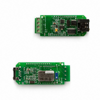
Manufacturer Part Number
RN-800S-CB
Description
MODULE A/D BLUETOOTH BLUESENTRY
Manufacturer
Roving Networks Inc
Specifications of RN-800S-CB
Frequency
2.4GHz
Modulation Or Protocol
Bluetooth v2.0, Class 1
Applications
Sensor Interface - Ready To Go Module
Power - Output
15dBm
Voltage - Supply
6 V ~ 12 V
Data Interface
PCB, Surface Mount
Antenna Connector
PCB, Surface Mount
Package / Case
Module
Antenna
Chip Antenna
Board Size
1.6 in x 3 in x 0.9 in
Lead Free Status / RoHS Status
Lead free / RoHS Compliant
Operating Temperature
-
Sensitivity
-
Memory Size
-
Data Rate - Maximum
-
Current - Transmitting
-
Current - Receiving
-
Lead Free Status / Rohs Status
Lead free / RoHS Compliant
Other names
740-1011


FIGURE 9. Histogram of 5,000 Conversions of a DC Input at the
FIGURE 10. Histogram of 5,000 Conversions of a DC Input at the
FIGURE 11. Histogram of 5,000 Conversions of a DC Input at the
AVERAGING
The noise of the A/D converter can be compensated by
averaging the digital codes. By averaging conversion results,
transition noise will be reduced by a factor of 1/ n, where n
is the number of averages. For example, averaging 4 conver-
14
Code Center, 5V operation internal clock mode.
Code Transition, 2.7V operation external clock mode.
Code Center, 2.7V operation internal clock mode.
7FFD
7FFD
7FFD
50
78
0
7FFE
7FFE
7FFE
251
666
858
7FFF
Code
7FFF
Code
7FFF
Code
3511
2868
4507
8000
8000
1137
8000
721
242
8001
8001
8001
52
59
0
sion results will reduce the transition noise by 1/2 to 0.25
LSBs. Averaging should only be used for input signals with
frequencies near DC.
For AC signals, a digital filter can be used to low-pass filter
and decimate the output codes. This works in a similar
manner to averaging: for every decimation by 2, the
signal-to-noise ratio will improve 3dB.
LAYOUT
For optimum performance, care should be taken with the
physical layout of the ADS8344 circuitry. This is particu-
larly true if the reference voltage is LOW and/or the conver-
sion rate is HIGH.
The basic SAR architecture is sensitive to glitches or sudden
changes on the power supply, reference, ground connec-
tions, and digital inputs that occur just prior to latching the
output of the analog comparator. Thus, during any single
conversion for an n-bit SAR converter, there are n “win-
dows” in which large external transient voltages can easily
affect the conversion result. Such glitches might originate
from switching power supplies, nearby digital logic, and
high-power devices. The degree of error in the digital output
depends on the reference voltage, layout, and the exact
timing of the external event. The error can change if the
external event changes in time with respect to the DCLK
input.
With this in mind, power to the ADS8344 should be clean
and well bypassed. A 0.1 F ceramic bypass capacitor should
be placed as close to the device as possible. In addition, a
1 F to 10 F capacitor and a 5
be used to low-pass filter a noisy supply.
The reference should be similarly bypassed with a 0.1 F
capacitor. Again, a series resistor and large capacitor can be
used to low-pass filter the reference voltage. If the reference
voltage originates from an op amp, make sure that it can
drive the bypass capacitor without oscillation (the series
resistor can help in this case). The ADS8344 draws very
little current from the reference on average, but it does place
larger demands on the reference circuitry over short periods
of time (on each rising edge of DCLK during a conversion).
The ADS8344 architecture offers no inherent rejection of
noise or voltage variation in regards to the reference input.
This is of particular concern when the reference input is tied
to the power supply. Any noise and ripple from the supply
will appear directly in the digital results. While
high-frequency noise can be filtered out as discussed in the
previous paragraph, voltage variation due to line frequency
(50Hz or 60Hz) can be difficult to remove.
The GND pin should be connected to a clean ground point.
In many cases, this will be the “analog” ground. Avoid
connections which are too near the grounding point of a
microcontroller or digital signal processor. If needed, run a
ground trace directly from the converter to the power-supply
entry point. The ideal layout will include an analog ground
plane dedicated to the converter and associated analog
circuitry.
or 10 series resistor may
ADS8344
SBAS139B
Related parts for RN-800S-CB
Image
Part Number
Description
Manufacturer
Datasheet
Request
R

Part Number:
Description:
MODULE BLUETOOTH SENSOR SMA
Manufacturer:
Roving Networks Inc
Datasheet:

Part Number:
Description:
Spacer
Manufacturer:
SPC TECHNOLOGY
Datasheet:

Part Number:
Description:
Spacer
Manufacturer:
SPC TECHNOLOGY
Datasheet:

Part Number:
Description:
Spacer
Manufacturer:
SPC TECHNOLOGY
Datasheet:

Part Number:
Description:
Spacer
Manufacturer:
SPC TECHNOLOGY
Datasheet:

Part Number:
Description:
Spacer
Manufacturer:
SPC TECHNOLOGY
Datasheet:

Part Number:
Description:
RES MF 1/8W 10.8K OHM 1% AXIAL
Manufacturer:
Stackpole Electronics Inc
Datasheet:
Part Number:
Description:
RES MF 1/8W 9.9K OHM 1% AXIAL
Manufacturer:
Stackpole Electronics Inc
Datasheet:

Part Number:
Description:
CONV DC/DC 1.25W 05VIN 09VOUT
Manufacturer:
Recom Power Inc
Datasheet:
Part Number:
Description:
CONV DC/DC 1.25W 05VIN 12VOUT
Manufacturer:
Recom Power Inc
Datasheet:
Part Number:
Description:
CONV DC/DC 1.25W 09VIN 15VOUT
Manufacturer:
Recom Power Inc
Datasheet:
Part Number:
Description:
CONV DC/DC 1.25W 09VIN 24VOUT
Manufacturer:
Recom Power Inc
Datasheet:

Part Number:
Description:
MODULE SOCKET BLUETOOTH CLASS1
Manufacturer:
Roving Networks Inc
Datasheet:

Part Number:
Description:
MODULE BLUETOOTH V2.1+EDR
Manufacturer:
Roving Networks Inc
Datasheet: