RN-800S-CB Roving Networks Inc, RN-800S-CB Datasheet - Page 2
RN-800S-CB
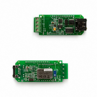
Manufacturer Part Number
RN-800S-CB
Description
MODULE A/D BLUETOOTH BLUESENTRY
Manufacturer
Roving Networks Inc
Specifications of RN-800S-CB
Frequency
2.4GHz
Modulation Or Protocol
Bluetooth v2.0, Class 1
Applications
Sensor Interface - Ready To Go Module
Power - Output
15dBm
Voltage - Supply
6 V ~ 12 V
Data Interface
PCB, Surface Mount
Antenna Connector
PCB, Surface Mount
Package / Case
Module
Antenna
Chip Antenna
Board Size
1.6 in x 3 in x 0.9 in
Lead Free Status / RoHS Status
Lead free / RoHS Compliant
Operating Temperature
-
Sensitivity
-
Memory Size
-
Data Rate - Maximum
-
Current - Transmitting
-
Current - Receiving
-
Lead Free Status / Rohs Status
Lead free / RoHS Compliant
Other names
740-1011


ABSOLUTE MAXIMUM RATINGS
PACKAGE/ORDERING INFORMATION
NOTE: (1) Stresses above those listed under “Absolute Maximum Ratings”
may cause permanent damage to the device. Exposure to absolute
maximum conditions for extended periods may affect device reliability.
NOTE: (1) Models with a slash (/) are available only in Tape and Reel in the quantities indicated (e.g., /2K5 indicates 2500 devices per reel). Ordering 2500 pieces
of “ADS8344E/2K5” will get a single 2500-piece Tape and Reel.
PIN CONFIGURATION
2
Top View
+V
Analog Inputs to GND ............................................ –0.3V to +V
Digital Inputs to GND ........................................................... –0.3V to +6V
Power Dissipation .......................................................................... 250mW
Maximum Junction Temperature ................................................... +150 C
Operating Temperature Range ........................................ –40 C to +85 C
Storage Temperature Range ......................................... –65 C to +150 C
Lead Temperature (soldering, 10s) ............................................... +300 C
PRODUCT
ADS8344E
ADS8344N
ADS8344EB
ADS8344NB
CC
to GND ........................................................................ –0.3V to +6V
"
"
"
"
SHDN
COM
CH0
CH1
CH2
CH3
CH4
CH5
CH6
CH7
10
1
2
3
4
5
6
7
8
9
ACCURACY
RELATIVE
MINIMUM
(LSB)
8
6
"
"
"
"
"
"
ADS8344
GAIN ERROR
MAXIMUM
0.024
(1)
(%)
0.05
"
"
"
"
"
"
20
19
18
17
16
15
14
13
12
11
+V
DCLK
CS
D
BUSY
D
GND
GND
+V
V
REF
IN
OUT
CC
CC
SPECIFICATION
TEMPERATURE
CC
–40 C to +85 C
–40 C to +85 C
+ 0.3V
RANGE
SSOP
"
"
"
"
"
"
PIN DESCRIPTIONS
This integrated circuit can be damaged by ESD. Texas Instru-
ments recommends that all integrated circuits be handled with
appropriate precautions. Failure to observe proper handling
and installation procedures can cause damage.
ESD damage can range from subtle performance degradation
to complete device failure. Precision integrated circuits may
be more susceptible to damage because very small parametric
changes could cause the device not to meet its published
specifications.
PIN
10
11
12
13
14
15
16
17
18
19
20
1
2
3
4
5
6
7
8
9
PACKAGE
QSOP-20
QSOP-20
SSOP-20
SSOP-20
"
"
"
"
NAME
SHDN
BUSY
DCLK
COM
+V
GND
GND
D
+V
V
CH0
CH1
CH2
CH3
CH4
CH5
CH6
CH7
D
CS
ELECTROSTATIC
DISCHARGE SENSITIVITY
REF
OUT
IN
CC
CC
DESCRIPTION
Analog Input Channel 0.
Analog Input Channel 1.
Analog Input Channel 2.
Analog Input Channel 3.
Analog Input Channel 4.
Analog Input Channel 5.
Analog Input Channel 6.
Analog Input Channel 7.
Ground reference for analog inputs. Sets zero code
voltage in single ended mode. Connect this pin to ground
or ground reference point.
Shutdown. When LOW, the device enters a very
low-power shutdown mode.
Voltage Reference Input. See Specification Table for
ranges.
Power Supply, 2.7V to 5V.
Ground.
Ground.
Serial Data Output. Data is shifted on the falling edge of
DCLK. This output is high impedance when CS is HIGH.
Busy Output. Busy goes LOW when the D
are being read and also when the device is converting.
The Output is high impedance when CS is HIGH.
Serial Data Input. If CS is LOW, data is latched on rising
edge of D
Chip Select Input. Active LOW. Data will not be clocked
into D
high impedance.
External Clock Input. The clock speed determines the
conversion rate by the equation f
Power Supply.
PACKAGE
DRAWING
NUMBER
349
334
349
334
"
"
"
"
IN
unless CS is LOW. When CS is HIGH, D
CLK
.
ADS8344EB/2K5
ADS8344NB/1K
ADS8344E/2K5
ADS8344N/1K
ADS8344EB
ADS8344NB
ORDERING
NUMBER
ADS8344N
ADS8344E
(1)
DCLK
= 24 • f
Tape and Reel
Tape and Reel
Tape and Reel
Tape and Reel
ADS8344
TRANSPORT
IN
SBAS139B
MEDIA
control bits
Rails
Rails
Rails
Rails
SAMPLE
OUT
.
is
Related parts for RN-800S-CB
Image
Part Number
Description
Manufacturer
Datasheet
Request
R

Part Number:
Description:
MODULE BLUETOOTH SENSOR SMA
Manufacturer:
Roving Networks Inc
Datasheet:

Part Number:
Description:
Spacer
Manufacturer:
SPC TECHNOLOGY
Datasheet:

Part Number:
Description:
Spacer
Manufacturer:
SPC TECHNOLOGY
Datasheet:

Part Number:
Description:
Spacer
Manufacturer:
SPC TECHNOLOGY
Datasheet:

Part Number:
Description:
Spacer
Manufacturer:
SPC TECHNOLOGY
Datasheet:

Part Number:
Description:
Spacer
Manufacturer:
SPC TECHNOLOGY
Datasheet:

Part Number:
Description:
RES MF 1/8W 10.8K OHM 1% AXIAL
Manufacturer:
Stackpole Electronics Inc
Datasheet:
Part Number:
Description:
RES MF 1/8W 9.9K OHM 1% AXIAL
Manufacturer:
Stackpole Electronics Inc
Datasheet:

Part Number:
Description:
CONV DC/DC 1.25W 05VIN 09VOUT
Manufacturer:
Recom Power Inc
Datasheet:
Part Number:
Description:
CONV DC/DC 1.25W 05VIN 12VOUT
Manufacturer:
Recom Power Inc
Datasheet:
Part Number:
Description:
CONV DC/DC 1.25W 09VIN 15VOUT
Manufacturer:
Recom Power Inc
Datasheet:
Part Number:
Description:
CONV DC/DC 1.25W 09VIN 24VOUT
Manufacturer:
Recom Power Inc
Datasheet:

Part Number:
Description:
MODULE SOCKET BLUETOOTH CLASS1
Manufacturer:
Roving Networks Inc
Datasheet:

Part Number:
Description:
MODULE BLUETOOTH V2.1+EDR
Manufacturer:
Roving Networks Inc
Datasheet: