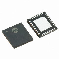
MRF89XA-I/MQ Microchip Technology, MRF89XA-I/MQ Datasheet - Page 9

MRF89XA-I/MQ
Manufacturer Part Number
MRF89XA-I/MQ
Description
TXRX ISM SUB-GHZ ULP 32QFN
Manufacturer
Microchip Technology
Specifications of MRF89XA-I/MQ
Package / Case
32-WFQFN Exposed Pad
Frequency
863MHz ~ 870MHz, 902MHz ~ 928MHz, 950MHz ~ 960MHz
Data Rate - Maximum
200kbps
Modulation Or Protocol
FSK, OOK
Applications
ISM
Power - Output
12.5dBm
Sensitivity
-113dBm
Voltage - Supply
2.1 V ~ 3.6 V
Current - Receiving
3mA
Current - Transmitting
25mA
Data Interface
PCB, Surface Mount
Antenna Connector
PCB, Surface Mount
Operating Temperature
-40°C ~ 85°C
Number Of Receivers
1
Number Of Transmitters
1
Wireless Frequency
863 MHz to 870 MHz, 902 MHz to 928 MHz, 950 MHz to 960 MHz
Interface Type
SPI
Noise Figure
- 112 dBc
Output Power
- 8.5 dBm, + 12.5 dBm
Operating Supply Voltage
2.1 V to 3.6 V
Maximum Operating Temperature
+ 85 C
Mounting Style
SMD/SMT
Maximum Data Rate
256 Kbps
Maximum Supply Current
25 mA
Minimum Operating Temperature
- 40 C
Modulation
FSK
Lead Free Status / RoHS Status
Lead free / RoHS Compliant
Memory Size
-
Lead Free Status / Rohs Status
Lead free / RoHS Compliant
Available stocks
Company
Part Number
Manufacturer
Quantity
Price
Company:
Part Number:
MRF89XA-I/MQ
Manufacturer:
MICROCHIP
Quantity:
12 000
2.0
The MRF89XA is an integrated, single chip, low-power
ISM band sub-GHz transceiver. A simplified architec-
tural block diagram of the MRF89XA is shown in
Figure 2-1. The frequency synthesizer is clocked by an
external 12.8 crystal, and frequency ranges from
863-870 MHz, 902-928 MHz and 950-960 MHz.
The MRF89XA receiver employs a super-heterodyne
architecture. Here, the first IF is 1/9th of the RF
frequency (approximately 100 MHz). The second down
conversion down converts the I and Q signals to base-
band in the case of the FSK receiver (Zero IF) and to a
low-IF (IF2) for the OOK receiver. After the second
down-conversion stage, the received signal is channel
select filtered and amplified to a level adequate for
demodulation. Both FSK and OOK demodulation are
available. Image rejection is achieved by the SAW filter.
The baseband I and Q signals at the transmitter side are
digitally generated by a DDS whose Digital-to-Analog
Converters (DAC) followed by two anti-aliasing low-pass
filters transform the digital signal into analog In-Phase (I)
and Quadrature (Q) components whose frequency is the
selected Frequency Deviation (Fdev). The transmitter
supports both FSK and OOK modes of operation. The
transmitter has a typical output power of +12.5 dBm. An
2010 Microchip Technology Inc.
HARDWARE DESCRIPTION
Advance Information
internal transmit/receive switch combines the transmitter
and receiver circuits into a single-ended RFIO pin. This
pin is connected to the impedance matching circuitry
(Balun) and to the external antenna with power amplifier
pin, if required. The device operates in the low-voltage
range of 2.1V to 3.6V, and in Sleep mode, it operates at
a very low-current state, typically 0.1 µA.
The quality of the data is validated using the RSSI and
bit synchronizer blocks built into the transceiver. Data
is buffered in 64-byte transmitter registers and receiver
FIFOs. The frequency synthesizer allows the use of a
low-accuracy, low-cost crystal. CLKOUT can be used
to clock the external controller. The transceiver is con-
trolled via a 4-wire Serial Peripheral Interface (SPI),
interrupt (IRO0 and IRO1), PLOCK, DATA and Chip
Select pins for SPI.
The MRF89XA supports the following feature blocks:
• Data Filtering and Whitening
• Bit Synchronization
• 64-Byte Transmit and Receive FIFO Buffer
• General Configuration Registers
These features reduce the processing load, which
allows the use of simple, low-cost 8-bit microcontrollers
for data processing.
MRF89XA
DS70622A-page 9


