CSM56F801SLK Freescale Semiconductor, CSM56F801SLK Datasheet - Page 9
CSM56F801SLK
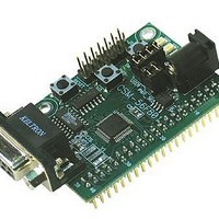
Manufacturer Part Number
CSM56F801SLK
Description
KIT LEARNING DSP 16BIT CSM56F801
Manufacturer
Freescale Semiconductor
Datasheet
1.CSM56F801SLK.pdf
(13 pages)
Specifications of CSM56F801SLK
Processor To Be Evaluated
DSP56F801
Data Bus Width
16 bit
Interface Type
RS-232
Lead Free Status / RoHS Status
Lead free / RoHS Compliant


D O C - 0 3 3 4 - 0 1 0 ,
Timing
The MPU function from either an internal relaxation oscillator or an external timing source. A
location for an external timing source has been provided. Component size for the external
timing source is based on an 8 MHz ceramic resonator from Panasonic, P/N EFO-S8004E5A.
This part is not populated in the default module configuration. Refer to the MPU User Guide for
further details
Communications
The CSM-56F801 module provides a single RS-232 communications port. An RS-232
transceiver (U2) provides RS-232 signal level to TTL/CMOS logic level translation on the first
RS-232 channel. RS232 signals TXD0 and RXD0 are routed between the transceiver and the
MCU. These signals are also routed to connector J1. RS-232 communication signals input on
J1 must be TTL/CMOS logic levels; no translation support is provided through this path. The
transceiver output may also be driven off-module if the signals are suitably buffered. As added
development support, hardware flow control signals RTS and CTS are available on the logic
side of U2. These signals are routed to vias located near the transceiver (U2). RTS has been
biased properly to support 2-wire RS-232 communications.
Use of the J1 connector to input RS-232 signals requires disabling the on-board RS-232
transceiver. Otherwise, signal corruption may occur. Disabling the on-board transceiver is
accomplished by opening cut-traces CT4, and CT5. Simply remove the circuit trace between
the cut-trace pads to open the circuit. To restore the circuit functionality, install a 1206 size, 0-
ohm, resistor or a short piece of wire across the cut-trace pads.
Table 3: COM Signal Connections
COM Connector
A standard 9-pin Dsub connector provides external connections for the COM port. The COM
port is used by default with the debug monitor. Component U2 provides RS-232 translation
services. The figure below details the DB9 connector.
COM Signal
R E V
RXD0
TXD0
D
Freescale Semiconductor, Inc.
GPIOB1/RXD0
GPIOB0/TXD0
MPU Port
9
Connector
J1
5
7
Disable
Signal
CT4
CT4
D E C E M B E R
2 ,
2 0 0 5
Related parts for CSM56F801SLK
Image
Part Number
Description
Manufacturer
Datasheet
Request
R

Part Number:
Description:
Manufacturer:
Freescale Semiconductor, Inc
Datasheet:
Part Number:
Description:
Manufacturer:
Freescale Semiconductor, Inc
Datasheet:
Part Number:
Description:
Manufacturer:
Freescale Semiconductor, Inc
Datasheet:
Part Number:
Description:
Manufacturer:
Freescale Semiconductor, Inc
Datasheet:
Part Number:
Description:
Manufacturer:
Freescale Semiconductor, Inc
Datasheet:
Part Number:
Description:
Manufacturer:
Freescale Semiconductor, Inc
Datasheet:
Part Number:
Description:
Manufacturer:
Freescale Semiconductor, Inc
Datasheet:
Part Number:
Description:
Manufacturer:
Freescale Semiconductor, Inc
Datasheet:
Part Number:
Description:
Manufacturer:
Freescale Semiconductor, Inc
Datasheet:
Part Number:
Description:
Manufacturer:
Freescale Semiconductor, Inc
Datasheet:
Part Number:
Description:
Manufacturer:
Freescale Semiconductor, Inc
Datasheet:
Part Number:
Description:
Manufacturer:
Freescale Semiconductor, Inc
Datasheet:
Part Number:
Description:
Manufacturer:
Freescale Semiconductor, Inc
Datasheet:
Part Number:
Description:
Manufacturer:
Freescale Semiconductor, Inc
Datasheet:
Part Number:
Description:
Manufacturer:
Freescale Semiconductor, Inc
Datasheet: