CSM56F801SLK Freescale Semiconductor, CSM56F801SLK Datasheet - Page 10
CSM56F801SLK
Manufacturer Part Number
CSM56F801SLK
Description
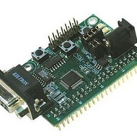
KIT LEARNING DSP 16BIT CSM56F801
Manufacturer
Freescale Semiconductor
Datasheet
1.CSM56F801SLK.pdf
(13 pages)
Specifications of CSM56F801SLK
Processor To Be Evaluated
DSP56F801
Data Bus Width
16 bit
Interface Type
RS-232
Lead Free Status / RoHS Status
Lead free / RoHS Compliant


D O C - 0 3 3 4 - 0 1 0 ,
Figure 2: COM Connector
User Options
Indicators LED1 and LED2 are connected to the MPU I/O ports by the USER option bank.
When the appropriate USER jumper is installed, the assigned LED is active. Each LED is
active low. A low voltage level driven out on the appropriate MPU port causes the LED to light.
MPU ports PWMA0 and PWMA1 drive LED1 and LED2 respectively.
Two push button switches provide momentary, active low, input to the MPU for user
applications. Switches SW1 and SW2 are connected to the MPU I/O ports by the USER
option bank. SW1 and SW2 provide input to MCUI/O ports TD0 and TD1 respectively. The
table below shows the user jumper settings.
Table 4: User Option Jumper Settings
I/O Connectors
JTAG / OnCE
The JTAG/OnCE 14 pin connector is compatible with the Freescale On Chip Emulation
(OnCE) development port. This connector allows the connection of a OnCE style background
debug cable for software development, programming and debugging in real-time.
GND 5
RXD 3
TXD 2
1
4
Jumper
User 1
User 2
User 3
User 4
6
7 RTS
8 CTS
9 NC
R E V
D
Freescale Semiconductor, Inc.
Female DB9 connector that interfaces to the MPU serial port
via the U2 RS232 transceiver. It provides simple 2 wire
asynchronous serial communications without flow control.
Flow control is provided at test points on the module.
Pins 1, 4, and 6 are connected together.
Enable LED1
Enable LED2
Enable SW1
Enable SW2
On
10
Disable LED1
Disable LED2
Disable SW1
Disable SW2
Off
MPU Signal
PWMA0
PWMA1
D E C E M B E R
TD0
TD1
2 ,
2 0 0 5
Related parts for CSM56F801SLK
Image
Part Number
Description
Manufacturer
Datasheet
Request
R

Part Number:
Description:
Manufacturer:
Freescale Semiconductor, Inc
Datasheet:
Part Number:
Description:
Manufacturer:
Freescale Semiconductor, Inc
Datasheet:
Part Number:
Description:
Manufacturer:
Freescale Semiconductor, Inc
Datasheet:
Part Number:
Description:
Manufacturer:
Freescale Semiconductor, Inc
Datasheet:
Part Number:
Description:
Manufacturer:
Freescale Semiconductor, Inc
Datasheet:
Part Number:
Description:
Manufacturer:
Freescale Semiconductor, Inc
Datasheet:
Part Number:
Description:
Manufacturer:
Freescale Semiconductor, Inc
Datasheet:
Part Number:
Description:
Manufacturer:
Freescale Semiconductor, Inc
Datasheet:
Part Number:
Description:
Manufacturer:
Freescale Semiconductor, Inc
Datasheet:
Part Number:
Description:
Manufacturer:
Freescale Semiconductor, Inc
Datasheet:
Part Number:
Description:
Manufacturer:
Freescale Semiconductor, Inc
Datasheet:
Part Number:
Description:
Manufacturer:
Freescale Semiconductor, Inc
Datasheet:
Part Number:
Description:
Manufacturer:
Freescale Semiconductor, Inc
Datasheet:
Part Number:
Description:
Manufacturer:
Freescale Semiconductor, Inc
Datasheet:
Part Number:
Description:
Manufacturer:
Freescale Semiconductor, Inc
Datasheet: