CSM56F801SLK Freescale Semiconductor, CSM56F801SLK Datasheet - Page 8
CSM56F801SLK
Manufacturer Part Number
CSM56F801SLK
Description
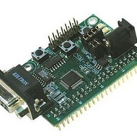
KIT LEARNING DSP 16BIT CSM56F801
Manufacturer
Freescale Semiconductor
Datasheet
1.CSM56F801SLK.pdf
(13 pages)
Specifications of CSM56F801SLK
Processor To Be Evaluated
DSP56F801
Data Bus Width
16 bit
Interface Type
RS-232
Lead Free Status / RoHS Status
Lead free / RoHS Compliant


D O C - 0 3 3 4 - 0 1 0 ,
PWR_SEL
The PWR_SEL jumper selects the source of power input to the DSP-56F801 module or allows
regulated +3.3VDC to be provided to J1 for use by external circuits. The module may be
powered from the 2.0mm barrel connector (PWR) or from the 40-pin MCU connector (J1).
Power input at the PWR jack must be DC voltage between +5V and +16V. Power input on the
MCU connector must be regulated voltage between +3.0VDC and +3.3VDC.
MCU_PORT connector input allows use of batteries, or other alternate sources, to power the
module. Damage may occur if the MCU_PORT power input pins are over-driven. Refer to the
table below to determine correct PWR_SEL jumper setting.
The PWR_SEL option jumper provides 3 possible configurations; source power from the PWR
connector, source power from J1, or source power from PWR and supply power to J1. The
figures below show the settings for each configuration.
Figure 1: PWR_SEL Jumper Settings
Reset Switch
The RESET switch provides a method to apply an asynchronous reset to the module.
Pressing the RESET switch applies a low voltage level to the RESET input. Logic on this
signal prevents unwanted RESET inputs to the MPU.
Low-Voltage Detect
The MPU includes an internal POR and Low-Voltage Interrupt circuit. This circuit protects
against low-voltage and under-voltage conditions. The system consists of a POR circuit and a
low-voltage interrupt (LVI) circuit.
reaches an acceptable level. The LVI provides an interrupt out when voltage falls below the
trip level. Refer to the MPU User Guide for further details.
CAUTION: Module damage may occur if the MCU_PORT power input pin (J1-1) is over-driven.
1
2
1
2
1
2
• •
• •
• •
• •
• •
• •
R E V
Module powered from external +3.0VDC - +3.3VDC input
connected to J1-1 (+) and J1-3 (-)
Module powered from external +5VDC - +16VDC connected to
PWR Terminal Block. J1-1 is open or not connected.
Module powered from external +3.0VVDC - +3.3VDC connected
to J1-1 (+) and J1-3 (-). Module provides +3.3VDC output (up to
50 mA) at pin J1 for use by external circuits.
D
Freescale Semiconductor, Inc.
The POR circuit holds the MPU in reset until voltage
8
D E C E M B E R
2 ,
2 0 0 5
The
Related parts for CSM56F801SLK
Image
Part Number
Description
Manufacturer
Datasheet
Request
R

Part Number:
Description:
Manufacturer:
Freescale Semiconductor, Inc
Datasheet:
Part Number:
Description:
Manufacturer:
Freescale Semiconductor, Inc
Datasheet:
Part Number:
Description:
Manufacturer:
Freescale Semiconductor, Inc
Datasheet:
Part Number:
Description:
Manufacturer:
Freescale Semiconductor, Inc
Datasheet:
Part Number:
Description:
Manufacturer:
Freescale Semiconductor, Inc
Datasheet:
Part Number:
Description:
Manufacturer:
Freescale Semiconductor, Inc
Datasheet:
Part Number:
Description:
Manufacturer:
Freescale Semiconductor, Inc
Datasheet:
Part Number:
Description:
Manufacturer:
Freescale Semiconductor, Inc
Datasheet:
Part Number:
Description:
Manufacturer:
Freescale Semiconductor, Inc
Datasheet:
Part Number:
Description:
Manufacturer:
Freescale Semiconductor, Inc
Datasheet:
Part Number:
Description:
Manufacturer:
Freescale Semiconductor, Inc
Datasheet:
Part Number:
Description:
Manufacturer:
Freescale Semiconductor, Inc
Datasheet:
Part Number:
Description:
Manufacturer:
Freescale Semiconductor, Inc
Datasheet:
Part Number:
Description:
Manufacturer:
Freescale Semiconductor, Inc
Datasheet:
Part Number:
Description:
Manufacturer:
Freescale Semiconductor, Inc
Datasheet: