AD6655-150EBZ Analog Devices Inc, AD6655-150EBZ Datasheet - Page 59
AD6655-150EBZ
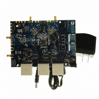
Manufacturer Part Number
AD6655-150EBZ
Description
BOARD EVAL FOR 150MSPS AD6655
Manufacturer
Analog Devices Inc
Type
Receiverr
Datasheet
1.AD6655-125EBZ.pdf
(88 pages)
Specifications of AD6655-150EBZ
Frequency
0Hz ~ 450MHz
Silicon Manufacturer
Analog Devices
Application Sub Type
IF Diversity Receiver
Kit Application Type
Communication & Networking
Silicon Core Number
AD6655
Kit Contents
Evaluation Board With AD6655 And Software
Lead Free Status / RoHS Status
Lead free / RoHS Compliant
For Use With/related Products
AD6655
Lead Free Status / RoHS Status
Lead free / RoHS Compliant, Lead free / RoHS Compliant


APPLICATIONS INFORMATION
DESIGN GUIDELINES
Before starting system-level design and layout of the AD6655,
it is recommended that the designer become familiar with these
guidelines, which discuss the special circuit connections and
layout requirements needed for certain pins.
Power and Ground Recommendations
When connecting power to the AD6655, it is recommended
that two separate 1.8 V supplies be used: one supply should be
used for analog (AVDD) and digital (DVDD), and a separate
supply should be used for the digital outputs (DRVDD). The
AVDD and DVDD supplies, while derived from the same source,
should be isolated with a ferrite bead or filter choke and separate
decoupling capacitors. The designer can employ several different
decoupling capacitors to cover both high and low frequencies.
These capacitors should be located close to the point of entry
at the PC board level and close to the pins of the part with
minimal trace length.
A single PCB ground plane should be sufficient when using the
AD6655. With proper decoupling and smart partitioning of the
PCB analog, digital, and clock sections, optimum performance
is easily achieved.
f
Because the AD6655 output data rate is at one-half the sampling
frequency, there is significant f
part. If this f
that this f
or the analog inputs of the AD6655. When f
in this fashion, it appears as a spurious tone reflected around f
3f
application with a 90 MHz single-tone analog input, this energy
generates a tone at 97.5 MHz. In this example, the center of the
Nyquist zone is 93.75 MHz; therefore, the 90 MHz input signal is
3.75 MHz from the center of the Nyquist zone. As a result, the f
spurious tone appears at 97.5 MHz, or 3.75 MHz above the center
of the Nyquist zone. These frequencies are then tuned by the NCOs
before being output by the AD6655.
Depending on the relationship of the IF frequency to the center
of the Nyquist zone, this spurious tone may or may not exist in the
AD6655 output band. Some residual f
the AD6655, and the level of this spur is typically below the
level of the harmonics at clock rates of 125 MSPS and below.
Figure 82 shows a plot of the f
frequency for the AD6655-125. At sampling rates above
125 MSPS, the f
than the worst harmonic, as shown in Figure 83, which shows
the AD6655-150 f
S
/2 Spurious
S
/4, 5f
S
/4, and so on. For example, in a 125 MSPS sampling
S
/2 energy does not couple into either the clock circuit
S
/2 spur falls in band, care must be taken to ensure
S
/2 spur level increases and is at a higher level
S
/2 levels.
S
S
/2 spur level vs. analog input
/2 energy in the outputs of the
S
/2 energy is present in
S
/2 energy is coupled
S
Rev. A | Page 59 of 88
S
/2
/4,
For the specifications provided in Table 2, the f
band, is excluded from the SNR values. It is treated as a
harmonic, in terms of SNR. The f
SFDR and worst other specifications.
Operating the part with a 1.8 V DRVDD voltage rather than a 3.3 V
DRVDD lowers the f
interleaved, or CMOS IQ output modes also reduces the f
spurious level.
LVDS Operation
The AD6655 defaults to CMOS output mode on power-up.
If LVDS operation is desired, this mode must be programmed
using the SPI configuration registers after power-up. When the
AD6655 powers up in CMOS mode with LVDS termination
resistors (100 Ω) on the outputs, the DRVDD current can be
higher than the typical value until the part is placed in LVDS
mode. This additional DRVDD current does not cause damage
to the AD6655, but it should be taken into account when consid-
ering the maximum DRVDD current for the part.
Figure 82. AD6655-125 SFDR and f
Figure 83. AD6655-150 SFDR and f
–100
–110
–120
–100
–110
–120
–60
–70
–80
–90
–60
–70
–80
–90
0
0
with DRVDD = 1.8 V Parallel CMOS Output Mode
with DRVDD = 1.8 V Parallel CMOS Output Mode
f
S
50
50
/2 SPUR
f
S
–SFDR
–SFDR
/2 SPUR
100
100
S
ANALOG INPUT FREQUENCY (MHz)
/2 spur. In addition, using LVDS, CMOS
150
150
INPUT FREQUENCY (MHz)
200
200
S
S
/2 Spurious Level vs. Input Frequency (f
/2 Spurious Level vs. Input Frequency (f
S
250
250
/2 level is included in the
300
300
350
350
S
/2 spur, if in
400
400
AD6655
450
450
500
500
S
/2
IN
IN
)
)
Related parts for AD6655-150EBZ
Image
Part Number
Description
Manufacturer
Datasheet
Request
R

Part Number:
Description:
BOARD EVAL W/AD6655 & SOFTWARE
Manufacturer:
Analog Devices Inc
Datasheet:

Part Number:
Description:
±1.7g Dual-Axis IMEMS Accelerometer Evaluation Board
Manufacturer:
Analog Devices Inc
Datasheet:

Part Number:
Description:
Inertial Sensor Evaluation System
Manufacturer:
Analog Devices Inc
Datasheet:
Part Number:
Description:
Manufacturer:
Analog Devices Inc
Datasheet:
Part Number:
Description:
Manufacturer:
Analog Devices Inc
Datasheet:
Part Number:
Description:
Manufacturer:
Analog Devices Inc
Datasheet:
Part Number:
Description:
Manufacturer:
Analog Devices Inc
Datasheet:
Part Number:
Description:
Manufacturer:
Analog Devices Inc
Datasheet:
Part Number:
Description:
Manufacturer:
Analog Devices Inc
Datasheet:
Part Number:
Description:
Manufacturer:
Analog Devices Inc
Datasheet:
Part Number:
Description:
Manufacturer:
Analog Devices Inc
Datasheet:
Part Number:
Description:
Manufacturer:
Analog Devices Inc
Datasheet:
Part Number:
Description:
Manufacturer:
Analog Devices Inc
Datasheet: