AD6655-150EBZ Analog Devices Inc, AD6655-150EBZ Datasheet
AD6655-150EBZ
Specifications of AD6655-150EBZ


Related parts for AD6655-150EBZ


AD6655-150EBZ Summary of contents
Page 1
... DATA INTERFACE FD[0:3]B SMI SMI SDFS SCLK/ PDWN Figure 1. One Technology Way, P.O. Box 9106, Norwood, MA 02062-9106, U.S.A. Tel: 781.329.4700 Fax: 781.461.3113 IF Diversity Receiver AD6655 DVDD DRVDD AD6655 D13A D0A CLK+ DIVIDE CLK– ADC NCO DUTY DCOA DCO CYCLE GENERATION ...
Page 2
... General Description ......................................................................... 4 Specifications ..................................................................................... 5 ADC DC Specifications—AD6655BCPZ-80/ AD6655BCPZ-105 ......................................................................... 5 ADC DC Specifications—AD6655BCPZ-125/ AD6655BCPZ-150 ......................................................................... 6 ADC AC Specifications—AD6655BCPZ-80/ AD6655BCPZ-105 ......................................................................... 7 ADC AC Specifications—AD6655BCPZ-125/ AD6655BCPZ-150 ......................................................................... 8 Digital Specifications—AD6655BCPZ-80/AD6655BCPZ-105 .. 9 Digital Specifications—AD6655BCPZ-125/ AD6655BCPZ-150 ....................................................................... 11 Switching Specifications—AD6655BCPZ-80/ AD6655BCPZ-105 ....................................................................... 13 Switching Specifications—AD6655BCPZ-125/ AD6655BCPZ-150 ....................................................................... 14 Timing Specifications ................................................................ 15 Absolute Maximum Ratings .......................................................... 18 Thermal Characteristics ............................................................ 18 ESD Caution ...
Page 3
... Added Exposed Pad Notation to Figure 9 and Table 12 ............ 19 Added Exposed Pad Notation to Figure 10 and Table 13 .......... 21 Updated Outline Dimensions ........................................................ 84 Changes to Ordering Guide ........................................................... 85 11/07—Revision 0: Initial Version Evaluation Board Layouts .......................................................... 74 Bill of Materials ........................................................................... 82 Outline Dimensions ........................................................................ 84 Ordering Guide ........................................................................... 85 Rev Page AD6655 ...
Page 4
... Flexible power-down options allow significant power savings, when desired. Programming for setup and control is accomplished using a 3-bit SPI-compatible serial interface. The AD6655 is available in a 64-lead LFCSP and is specified over the industrial temperature range of −40°C to +85°C. Rev Page ...
Page 5
... SPECIFICATIONS ADC DC SPECIFICATIONS—AD6655BCPZ-80/AD6655BCPZ-105 AVDD = 1.8 V, DVDD = 1.8 V, DRVDD = 1.8 V, maximum sample rate, VIN = −1.0 dBFS differential input, 1.0 V internal reference, DCS enabled, unless otherwise noted. Table 1. Parameter Temperature RESOLUTION Full ACCURACY No Missing Codes Full Offset Error Full Gain Error Full ...
Page 6
... AD6655 ADC DC SPECIFICATIONS—AD6655BCPZ-125/AD6655BCPZ-150 AVDD = 1.8 V, DVDD = 1.8 V, DRVDD = 1.8 V, maximum sample rate, VIN = −1.0 dBFS differential input, 1.0 V internal reference, DCS enabled, unless otherwise noted. Table 2. Parameter RESOLUTION ACCURACY No Missing Codes Offset Error Gain Error MATCHING CHARACTERISTIC Offset Error Gain Error ...
Page 7
... See Application Note AN-835, Understanding High Speed ADC Testing and Evaluation, for a complete set of definitions. 2 See the Applications Information section for more information about the worst other specifications for the AD6655. 3 Crosstalk is measured at 100 MHz with −1 dBFS on one channel and with no input on the alternate channel. AD6655BCPZ-80 ...
Page 8
... See Application Note AN-835, Understanding High Speed ADC Testing and Evaluation, for a complete set of definitions. 2 See the Applications Information section for more information about the worst other specifications for the AD6655. 3 Crosstalk is measured at 100 MHz with −1 dBFS on one channel and with no input on the alternate channel. AD6655BCPZ-125 ...
Page 9
... DIGITAL SPECIFICATIONS—AD6655BCPZ-80/AD6655BCPZ-105 AVDD = 1.8 V, DVDD = 1.8 V, DRVDD = 1.8 V, maximum sample rate, VIN = DCS enabled, unless otherwise noted. Table 5. Parameter DIFFERENTIAL CLOCK INPUTS (CLK+, CLK−) Logic Compliance Internal Common-Mode Bias Differential Input Voltage Input Voltage Range Input Common-Mode Range High Level Input Voltage ...
Page 10
... Full 1.75 Full 0.2 Full 0.05 Full 250 350 450 Full 1.15 1.25 1.35 Full 150 200 280 Full 1.15 1.25 1.35 Full Rev Page AD6655BCPZ-105 Min Typ Max Unit 1.22 3 0.6 V −90 −134 μA −10 +10 μA 26 kΩ 3. ...
Page 11
... DIGITAL SPECIFICATIONS—AD6655BCPZ-125/AD6655BCPZ-150 AVDD = 1.8 V, DVDD = 1.8 V, DRVDD = 1.8 V, maximum sample rate, VIN = −1.0 dBFS differential input, 1.0 V internal reference, DCS enabled, unless otherwise noted. Table 6. Parameter DIFFERENTIAL CLOCK INPUTS (CLK+, CLK−) Logic Compliance Internal Common-Mode Bias Differential Input Voltage ...
Page 12
... Full 0.2 Full 0.05 Full 250 350 450 Full 1.15 1.25 1.35 Full 150 200 280 Full 1.15 1.25 1.35 Rev Page AD6655BCPZ-150 Min Typ Max 1.22 3.6 0 0.6 −90 −134 −10 + 3.29 3.25 0.2 0.05 1.79 1.75 0.2 0.05 ...
Page 13
... SWITCHING SPECIFICATIONS—AD6655BCPZ-80/AD6655BCPZ-105 Table 7. Parameter CLOCK INPUT PARAMETERS Input Clock Rate 1 Conversion Rate DCS Enabled DCS Disabled CLK Period—Divide-by-1 Mode (t ) CLK CLK Pulse Width High (t ) CLKH Divide-by-1 Mode, DCS Enabled Divide-by-1 Mode DCS Disabled Divide-by-2 Mode, DCS Enabled Divide-by-3 Through Divide-by-8 Modes, DCS Enabled DATA OUTPUT PARAMETERS (DATA, FD) CMOS Noninterleaved Mode— ...
Page 14
... AD6655 SWITCHING SPECIFICATIONS—AD6655BCPZ-125/AD6655BCPZ-150 Table 8. Parameter CLOCK INPUT PARAMETERS Input Clock Rate 1 Conversion Rate DCS Enabled DCS Disabled CLK Period—Divide-by-1 Mode (t ) CLK CLK Pulse Width High (t ) CLKH Divide-by-1 Mode, DCS Enabled Divide-by-1 Mode, DCS Disabled Divide-by-2 Mode, DCS Enabled Divide-by-3 Through Divide-by-8 Modes, DCS Enabled DATA OUTPUT PARAMETERS (DATA, FD) CMOS Noninterleaved Mode— ...
Page 15
... DCO CHANNEL A/B CHANNEL A/B DATA BITS DATA BITS CHANNEL A/B CHANNEL A/B FD BITS FD BITS t DCO CHANNEL A/B CHANNEL A/B DATA BITS DATA BITS CHANNEL A/B CHANNEL A/B FD BITS FD BITS AD6655 Max Unit 6.2 ns +0.4 ns +0.4 ns ...
Page 16
... AD6655 CLK DECIMATED CHANNEL A: CHANNEL B: INTERLEAVED DATA CMOS DATA DECIMATED CHANNEL A: CHANNEL B: INTERLEAVED FD BITS FD DATA DECIMATED DCO Figure 4. Decimated Interleaved CMOS Mode Data and Fast Detect Output Timing CLK CHANNEL A/B: DECIMATED Q DATA CMOS IQ OUTPUT DATA CHANNEL A/B: CMOS FD FD BITS ...
Page 17
... CLK+ CLK– t CSSCLK SMI SCLK t SSCLKSDFS SMI SDFS SMI SDO t SSCLKSDFS DATA Figure 8. Signal Monitor SPORT Output Timing Rev Page AD6655 DATA ...
Page 18
... AD6655 ABSOLUTE MAXIMUM RATINGS Table 10. Parameter ELECTRICAL AVDD, DVDD to AGND DRVDD to DRGND AGND to DRGND VIN+A/VIN+B, VIN-A/VIN−B to AGND CLK+, CLK− to AGND SYNC to AGND VREF to AGND SENSE to AGND CML to AGND RBIAS to AGND CSB to AGND SCLK/DFS to DRGND SDIO/DCS to DRGND SMI SDO/OEB to DRGND ...
Page 19
... Channel B Fast Detect Indicator. (See Table 21 for details.) Channel B Fast Detect Indicator. (See Table 21 for details.) Channel B Fast Detect Indicator. (See Table 21 for details.) Rev Page SCLK/DFS 47 SDIO/DCS 46 AVDD 45 AVDD 44 VIN+B 43 VIN–B 42 RBIAS 41 CML 40 SENSE 39 VREF 38 VIN–A 37 VIN+A 36 AVDD 35 SMI SDFS 34 SMI SCLK/PDWN 33 SMI SDO/OEB AD6655 ...
Page 20
... AD6655 Pin No. Mnemonic Type Digital Input 52 SYNC Input Digital Outputs 12 D0A (LSB) Output 13 D1A Output 14 D2A Output 15 D3A Output 16 D4A Output 17 D5A Output 18 D6A Output 19 D7A Output 22 D8A Output 23 D9A Output 25 D10A Output 26 D11A Output 27 D12A Output 28 D13A (MSB) Output 58 D0B (LSB) ...
Page 21
... Channel A/Channel B LVDS Fast Detect Indicator 3—True. See Table 21 for details. Channel A/Channel B LVDS Fast Detect Indicator 3—Complement. See Table 21 for details. Rev Page SCLK/DFS 47 SDIO/DCS 46 AVDD 45 AVDD 44 VIN+B 43 VIN–B 42 RBIAS 41 CML 40 SENSE 39 VREF 38 VIN–A 37 VIN+A 36 AVDD 35 SMI SDFS 34 SMI SCLK/PDWN 33 SMI SDO/OEB AD6655 ...
Page 22
... AD6655 Pin No. Mnemonic Type Digital Input 52 SYNC Input Digital Outputs 63 D0+ (LSB) Output 62 D0− (LSB) Output 3 D1+ Output 2 D1− Output 5 D2+ Output 4 D2− Output 7 D3+ Output 6 D3− Output 9 D4+ Output 8 D4− Output 13 D5+ Output 12 D5− ...
Page 23
... Figure 14. Equivalent SDIO/DCS Circuit or SMI SDFS Circuit . SCLK/DFS Figure 15. Equivalent SCLK/DFS Input Circuit SENSE CLK– Figure 16. Equivalent SENSE Circuit CSB Figure 17. Equivalent CSB Input Circuit Rev Page AD6655 1kΩ 26kΩ 1kΩ AVDD 26kΩ 1kΩ AVDD VREF 6kΩ Figure 18. Equivalent VREF Circuit ...
Page 24
... SNR = 71.8dBc (72.8dBFS) –20 SFDR = 81.4dBc f = 205MHz NCO –40 –60 THIRD HARMONIC –80 –100 –120 –140 FREQUENCY (MHz) Figure 23. AD6655-150 Single-Tone FFT with 205 MHz NCO 0 150MSPS 332.1MHz @ –1dBFS SNR = 71.7dBc (72.7dBFS) –20 SFDR = 95.0dBc f = 321.5MHz NCO –40 –60 –80 –100 –120 –140 ...
Page 25
... Figure 27. AD6655-125 Single-Tone FFT with 445.1 MHz 429 MHz Figure 28. AD6655-125 Single-Tone FFT with f NCO = 15.75MHz =2.4 MHz 15.75 MHz Figure 29. AD6655-125 Single-Tone FFT with f NCO THIRD HARMONIC 30.3 MHz MHz Figure 30. AD6655-125 Single-Tone FFT with f NCO Rev Page 125MSPS 70.3MHz @ –1dBFS SNR = 74.6dBc (75.6dBFS) – ...
Page 26
... REFERENCE LINE –3.5 –4.0 –30 –20 – with IN SFDR = +25°C 300 350 400 450 ) and Figure 36. AD6655-150 Two-Tone SFDR/IMD3 vs. Input Amplitude (A IN Rev Page SFDR = +85° SFDR = –40°C 75 SNR = +25°C 70 SNR = +85°C SNR = –40° 100 ...
Page 27
... SFDR (dBc) –40 IMD3 (dBc) –60 –80 IMD3 (dBFS) SFDR (dBFS) –100 –120 –90 –78 –66 –54 –42 INPUT AMPLITUDE (dBFS) Figure 37. AD6655-150 Two-Tone SFDR/IMD3 vs. Input Amplitude ( 169.12 MHz 172.12 MHz 150 MSPS, f IN1 IN2 S 0 –20 –40 –60 –80 –100 –120 – ...
Page 28
... SFDR DCS OFF 80 SNR DCS ON 75 SNR DCS OFF DUTY CYCLE (%) Figure 44. AD6655-150 SNR/SFDR vs. Duty Cycle with MHz NCO 0.85 LSB rms Figure 45. AD6655-150 SNR/SFDR vs. Input Common Mode ( 30.3 MHz, IN Rev Page SFDR 80 75 SNR 70 65 0.2 0.4 0.6 0.8 1.0 ...
Page 29
... V (approximately 1.6 V). CMREF Input Common Mode The analog inputs of the AD6655 are not internally dc biased. In ac-coupled applications, the user must provide this bias externally. Setting the device so that V recommended for optimum performance, but the device functions over a wider range with reasonable performance (see Figure 45). ...
Page 30
... ADA4938-2 provide excellent performance and a flexible interface to the ADC. The output common-mode voltage of the AD8138 is easily set with the CML pin of the AD6655 (see Figure 47), and the driver can be configured in a Sallen-Key filter topology to provide band limiting of the input signal. 499Ω ...
Page 31
... A stable and accurate voltage reference is built into the AD6655. The input range can be adjusted by varying the reference voltage applied to the AD6655, using either the internal reference or an externally applied reference voltage. The input span of the ADC tracks reference voltage changes linearly. The various reference modes are summarized in the sections that follow ...
Page 32
... Figure 57 and Figure 58 show two preferred methods for clocking 1.5 2.0 the AD6655 (at clock rates 625 MHz). A low jitter clock source is converted from a single-ended signal to a differential signal using an RF transformer. The back-to-back Schottky diodes across the transformer secondary limit clock excursions into the AD6655 to approximately 0 ...
Page 33
... CMOS DRIVER INPUT 50Ω 1kΩ Figure 62. Single-Ended 3.3 V CMOS Sample Clock (Up to 150 MSPS) Input Clock Divider The AD6655 contains an input clock divider with the ability to 0.1µF CLK+ divide the input clock by integer values between 1 and divide ADC 100Ω ...
Page 34
... Figure 63. SNR vs. Input Frequency and Jitter The clock input should be treated as an analog signal in cases where aperture jitter may affect the dynamic range of the AD6655. Power supplies for clock drivers should be separated from the ADC output driver supplies to avoid modulating the clock signal with digital noise ...
Page 35
... The length of the output data lines and loads placed on them should be minimized to reduce transients within the AD6655. These transients can degrade converter dynamic performance. The lowest typical conversion rate of the AD6655 is 10 MSPS. At clock rates below 10 MSPS, dynamic performance may degrade. Data Clock Output (DCO) The AD6655 also provides data clock output (DCO) intended for capturing the data in an external register ...
Page 36
... AD6655 Table 17. Output Data Format Input (V) Condition (V) VIN+ – VIN– < –VREF – 0.5 LSB VIN+ – VIN– = –VREF VIN+ – VIN– VIN+ – VIN– = +VREF – 1.0 LSB VIN+ – VIN– > +VREF – 0.5 LSB Offset Binary Output Mode ...
Page 37
... HALF-BAND DECIMATING FILTER AND FIR FILTER The goal of the AD6655 digital filter block is to allow the sample rate to be reduced by a factor of 2 while rejecting aliases that fall into the band of interest. The half-band filter is designed to operate ...
Page 38
... This processing stage comprises a digital tuner consisting of a 32-bit complex numerically controlled oscillator (NCO). The two channels of the AD6655 share a single NCO. The NCO is optional and can be bypassed by clearing Bit 0 of Register 0x11D. This NCO block accepts a real input from the ADC stage and outputs a frequency translated complex (I and Q) output ...
Page 39
... DECIMATING HALF-BAND FILTER AND FIR FILTER The goal of the AD6655 half-band digital filter is to allow the sample rate to be reduced by a factor of 2 while rejecting aliases that fall into the band of interest. This filter is designed to operate as either a low-pass or a high-pass filter and to provide >100 dB of alias protection for 11% of the input rate of the structure ...
Page 40
... The final NCO provides a −152696 −161248 means to move this complex output signal away from dc so that a real output can be provided from the AD6655. The final NCO, 337056 if enabled, translates the output from frequency equal to 922060 the ADC sampling frequency divided ...
Page 41
... FAST DETECT OVERVIEW The AD6655 contains circuitry to facilitate fast overrange detection, allowing very flexible external gain control imple- mentations. Each ADC has four fast detect (FD) output pins that are used to output information about the current state of the ADC input level ...
Page 42
... ADC clock cycles. An overrange at the input is indicated by this bit 12 clock cycles after it occurs. GAIN SWITCHING The AD6655 includes circuitry that is useful in applications either where large dynamic ranges exist or where gain ranging converters are employed. This circuitry allows digital thresholds to be set such that an upper threshold and a lower threshold can be programmed ...
Page 43
... The operation of the increment gain output and decrement gain output is shown graphically in Figure 75. DWELL TIME TIMER RESET BY RISE ABOVE F_LT Figure 75. Threshold Settings for C_UT, F_UT, F_LT, DG, and IG Rev Page UPPER THRESHOLD (COARSE OR FINE) FINE LOWER THRESHOLD TIMER COMPLETES BEFORE DWELL TIME SIGNAL RISES ABOVE F_LT AD6655 ...
Page 44
... AD6655 SIGNAL MONITOR The signal monitor block provides additional information about the signal being digitized by the ADC. The signal monitor computes the rms input magnitude, the peak magnitude, and/or the number of samples by which the magnitude exceeds a particular threshold. Together, these functions can be used to ...
Page 45
... GSM. Rev Page POWER MONITOR DOWN IS COUNT = 1? PERIOD REGISTER COUNTER LOAD LOAD CLEAR POWER MONITOR A COMPARE COMPARE HOLDING A>B A>B REGISTER B UPPER THRESHOLD REGISTER Figure 78. ADC Input Threshold Crossing Block Diagram AD6655 TO INTERRUPT CONTROLLER TO MEMORY MAP ...
Page 46
... Bits[5:2] of Register 0x10C (values between 0 and 13 are valid for k; programming provides the same result as programming 13 the AD6655 ADC sample rate in hertz (Hz). CLK DC Correction Readback The current dc correction value can be read back in Register 0x10D and Register 0x10E for Channel A and Register 0x10F and Register 0x110 for Channel B ...
Page 47
... CHANNEL/CHIP SYNCHRONIZATION The AD6655 has a SYNC input that allows the user flexible synchronization options for synchronizing the internal blocks. The sync feature is useful for guaranteeing synchronized operation across multiple ADCs. The input clock divider, NCO, half-band filters, and signal monitor block can be synchronized using the SYNC input ...
Page 48
... If the on-board SPI bus is used for other devices, it may be necessary to provide buffers between this bus and the AD6655 to prevent these signals from transi- tioning at the converter inputs during critical sampling periods. Some pins serve a dual function when the SPI interface is not being used ...
Page 49
... Table 28 provides a brief description of the general features that are accessible via the SPI. These features are described in detail in Application Note AN-877, Interfacing to High Speed ADCs via SPI (see www.analog.com). The AD6655 part-specific features are described in the Memory Map Register Description section. Table 28. Features Accessible Using the SPI ...
Page 50
... Address 0x18). If the entire address location is open (for example, Address 0x13), this address location should not be written. Default Values After the AD6655 is reset, critical registers are loaded with default values. The default values for the registers are given in the memory map register table, Table 29. Logic Levels An explanation of logic level terminology follows: • ...
Page 51
... Clock Divide Open Open (Global) Bit 5 Bit 4 Bit 3 Bit 2 Soft reset 1 1 Soft reset 8-bit Chip ID[7:0] (AD6655 = 0x0D) (default) Speed Grade ID[4:3] Open Open 00 = 150 MSPS 01 = 125 MSPS 10 = 105 MSPS MSPS Open Open Open Open Open Open Open ...
Page 52
... AD6655 Addr. Register Bit 7 Bit 6 (Hex) Name (MSB) 0x0D Test Mode Open Open (Local) 0x10 Offset Adjust Open Open (Local) 0x14 Output Mode Drive Output strength type 3 CMOS V CMOS LVDS ANSI (global) LVDS 1.8 V CMOS or reduced LVDS (global) 0x16 Open Clock Phase ...
Page 53
... DC Value Channel B[13:8] Peak Threshold SPORT SMI SCLK detector crossing divide output output 00 = Undefined enable enable 01 = divide divide divide by 8 Rev Page AD6655 Default Bit 0 Value Bit 1 (LSB) (Hex) Fast detect 0x00 enable Coarse Upper Threshold[2:0] 0x00 0x00 0x00 0x00 0x00 ...
Page 54
... AD6655 Addr. Register Bit 7 Bit 6 (Hex) Name (MSB) 0x112 Signal Complex Open Monitor power Control calculation (Global) mode enable 0x113 Signal Monitor Period Register 0 (Global) 0x114 Signal Monitor Period Register 1 (Global) 0x115 Signal Monitor Period Register 2 (Global) 0x116 Signal Monitor Result ...
Page 55
... When set high, Bit 0 enables the FIR filter. When Bit 0 is cleared, the FIR filter is bypassed and shut down for power savings. Rev Page Default Bit 0 Value Bit 1 (LSB) (Hex) 0x00 0x00 0x00 /8 Start State output mix when enabled. Bit 2 should be S AD6655 Default Notes/ Comments /8 S ...
Page 56
... Bits[5:2] of Register 0x10C (values between 0 and 13 are valid for k; programming provides the same result as programming 13 the AD6655 ADC sample rate in hertz (Hz). CLK Bit 1—DC Correction for Signal Path Enable Setting this bit high causes the output of the dc measurement block to be summed with the data in the signal path to remove the dc offset from the signal path ...
Page 57
... Bit 2—NCO32 Phase Dither Enable When Bit 2 is set, phase dither in the NCO is enabled. When Bit 2 is cleared, phase dither is disabled. Bit 1—NCO32 Amplitude Dither Enable When Bit 1 is set, amplitude dither in the NCO is enabled. When Bit 1 is cleared, amplitude dither is disabled. Rev Page AD6655 ...
Page 58
... NCO_FREQ is a 32-bit twos complement number representing the NCO frequency register the desired carrier frequency in hertz (Hz the AD6655 ADC clock rate in hertz (Hz). CLK NCO Phase Offset (Register 0x122 and Register 0x123) Register 0x122, Bits[7:0]—NCO Phase Value[7:0] Register 0x123, Bits[7:0]—NCO Phase Value[15:8] ...
Page 59
... DRVDD current can be higher than the typical value until the part is placed in LVDS mode. This additional DRVDD current does not cause damage to the AD6655, but it should be taken into account when consid- ering the maximum DRVDD current for the part. Rev Page ...
Page 60
... The CML pin should be decoupled to ground with a 0.1 μF capacitor, as shown in Figure 48. RBIAS The AD6655 requires that a 10 kΩ resistor be placed between the RBIAS pin and ground. This resistor sets the master current reference of the ADC core and should have at least a 1% tolerance. ...
Page 61
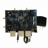
... EVALUATION BOARD The AD6655 evaluation board provides all of the support circuitry required to operate the ADC in its various modes and configura- tions. The converter can be driven differentially through a double balun configuration (default) or optionally through the AD8352 differential driver. The ADC can also be driven in a single-ended fashion ...
Page 62
... The transformer converts the single-ended input to a differential signal that is clipped before entering the ADC clock inputs. When the AD6655 input clock divider is utilized, clock frequencies up to 625 MHz can be input into the evaluation board through Connector S5. ...
Page 63
... Populate the optional amplifier output path with the desired components including an optional low-pass filter. Install 0 Ω resistors, R44 and R48. R43 and R47 should be increased (typically to 100 Ω) to increase to 200 Ω the output impedance seen by the AD8352. Rev Page AD6655 ...
Page 64
... AD6655 SCHEMATICS OHM 10K R41 OHM 100 7 R12 4.12K R126 DNP R36 OHM 24.9 OHM 24.9 R29 R35 F Figure 85. Evaluation Board Schematic, Channel A Analog Inputs Rev Page 06709-200 OHM 57.6 R5 OHM 33 OHM 33 R43 R47 OHM OHM 57.6 OHM 57.6 R1 R28 2 2 ...
Page 65
... M OH 10K R53 AMPVDD M OH 100 R129 4.12K R128 P DN R68 24.9 R134 R135 F Figure 86. Evaluation Board Schematic, Channel B Analog Inputs Rev Page 06709-201 M OH 57.6 R72 R70 R71 R69 57 57.6 R52 R51 2 2 AD6655 ...
Page 66
... AD6655 10KOHM 10KOHM R85 24.9OHM R83 F R82 OHM 0 R8 57.6OHM R30 2 Figure 87. Evaluation Board Schematic, DUT Clock Input Rev Page 06709-202 TP2 1 2 DNP R34 57.6OHM R7 2 ...
Page 67
... Figure 88. Evaluation Board Schematic, Optional AD9516 Clock Circuit Rev Page 06709-203 2 2 PAD VS_OUT89_ 2 32 VS_OUT89_ 1 31 VS_OUT45_DI OUT5 29 5 OUT 28 VS_OUT45_DR V R VS_OUT_D 27 B OUT4 26 4 OUT 25 PDB PDB 24 B RESET B RESET 23 SDIO SDI 22 SDO SDO 21 NC4 20 NC3 19 NC2 18 CSB 2 CSB_ 17 OHM 49.9 R89 2 AD6655 ...
Page 68
... AD6655 A C Figure 89. Evaluation Board Schematic, Optional AD9516 Loop Filter/VCO and SYNC Input RES0402 M OH 10K R105 RES0402 M OH 10K R103 RES0402 M OH 10K R102 RES0402 M OH 10K R100 RES0402 M OH 10K R107 RES0402 M OH 10K R106 M OH 24.9 R87 TP1 ...
Page 69
... D5A DRGND D6A D5B D7A D4B DRGND1 D3B DRVDD1 D2B D8A D1B D9A D0B_LSB_ DVDD1 DVDD2 D10A FD3B D11A FD2B D12A FD1B D13A_MSB_ FD0B FD0A SYNC FD1A SPI_CSB FD2A CLK- FD3A CLK+ Rev Page AD6655 709-205 DVDD SYNC 51 SPI_CSB 50 - CLK 49 + CLK ...
Page 70
... AD6655 10KOHM R118 2 RES040 VAL R130 2 RES040 10KOHM R140 Figure 91. Evaluation Board Schematic, Digital Output Interface Rev Page 06709-206 100OHM R77 ...
Page 71
... Figure 92. Evaluation Board Schematic, SPI Circuitry Rev Page AD6655 06709-207 2 RES040 10KOHM R65 ...
Page 72
... AD6655 GND 4 1 RES0603 M OH 261 A C R16 CR7 2 1 S2A_REC T M KOH 76 147K R13 R14 SJ35 Figure 93. Evaluation Board Schematic, Power Supply Rev Page 06709-208 1 TP25 ...
Page 73
... GND 4 1 SJ37 SJ36 GND GND Figure 94. Evaluation Board Schematic, Power Supply (Continued) Rev Page 140KOH M 78.7KOH R25 R15 AD6655 06709-209 ...
Page 74
... AD6655 EVALUATION BOARD LAYOUTS Figure 95. Evaluation Board Layout, Primary Side Rev Page ...
Page 75
... Figure 96. Evaluation Board Layout, Ground Plane Rev Page AD6655 ...
Page 76
... AD6655 Figure 97. Evaluation Board Layout, Power Plane Rev Page ...
Page 77
... Figure 98. Evaluation Board Layout, Power Plane Rev Page AD6655 ...
Page 78
... AD6655 Figure 99. Evaluation Board Layout, Ground Plane Rev Page ...
Page 79
... Figure 100. Evaluation Board Layout, Secondary Side (Mirrored Image) Rev Page AD6655 ...
Page 80
... AD6655 Figure 101. Evaluation Board Layout, Silkscreen, Primary Side Rev Page ...
Page 81
... Figure 102. Evaluation Board Layout, Silkscreen, Secondary Side Rev Page AD6655 ...
Page 82
... AD6655 BILL OF MATERIALS Table 30. Evaluation Board Bill of Materials (BOM) Reference Item Qty Designator Description 1 1 AD6655CE_REVB PCB C3, C6, C7, 0.1 μ ceramic C13, C14, C17, C18, capacitor, SMT 0402 C20 to C26, C32, C57 to C61, C65 to C76, C81 to C83, C96 to C101, C103, C105, C107, ...
Page 83
... R76 200 Ω, 0402, 1/ resistor 36 4 S2, S3, S5, S12 SMA, inline, male, coaxial connector 37 1 SJ35 0 Ω, 1 resistor Balun IC, AD6655 Clock distribution, PLL Dual inverter Dual buffer IC, open-drain circuits UHS dual buffer U15 to U17 16-bit CMOS buffer IC ...
Page 84
... AD6655 OUTLINE DIMENSIONS PIN 1 INDICATOR TOP VIEW 12° MAX 1.00 0.85 0.80 SEATING PLANE PIN 1 INDICATOR TOP VIEW 12° MAX 1.00 0.85 0.80 SEATING PLANE 9.00 BSC SQ 0.60 MAX 49 48 0.50 8.75 BSC BSC SQ 0.50 0. 0.30 0.80 MAX 0.65 TYP 0.05 MAX ...
Page 85
... AD6655BCPZ-80 −40°C to +85°C 1 AD6655-125EBZ 1 AD6655-150EBZ RoHS Compliant Part. Package Description 64-Lead Lead Frame Chip Scale Package [LFCSP_VQ] 64-Lead Lead Frame Chip Scale Package [LFCSP_VQ] 64-Lead Lead Frame Chip Scale Package [LFCSP_VQ] 64-Lead Lead Frame Chip Scale Package [LFCSP_VQ] ...
Page 86
... AD6655 NOTES Rev Page ...
Page 87
... NOTES Rev Page AD6655 ...
Page 88
... AD6655 NOTES ©2007–2009 Analog Devices, Inc. All rights reserved. Trademarks and registered trademarks are the property of their respective owners. D06709-0-9/09(A) Rev Page ...