AD6655-150EBZ Analog Devices Inc, AD6655-150EBZ Datasheet - Page 21
AD6655-150EBZ
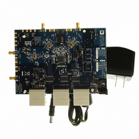
Manufacturer Part Number
AD6655-150EBZ
Description
BOARD EVAL FOR 150MSPS AD6655
Manufacturer
Analog Devices Inc
Type
Receiverr
Datasheet
1.AD6655-125EBZ.pdf
(88 pages)
Specifications of AD6655-150EBZ
Frequency
0Hz ~ 450MHz
Silicon Manufacturer
Analog Devices
Application Sub Type
IF Diversity Receiver
Kit Application Type
Communication & Networking
Silicon Core Number
AD6655
Kit Contents
Evaluation Board With AD6655 And Software
Lead Free Status / RoHS Status
Lead free / RoHS Compliant
For Use With/related Products
AD6655
Lead Free Status / RoHS Status
Lead free / RoHS Compliant, Lead free / RoHS Compliant


Table 13. Pin Function Descriptions (Interleaved Parallel LVDS Mode)
Pin No.
ADC Power Supplies
20, 64
1, 21
24, 57
36, 45, 46
0
ADC Analog
37
38
44
43
39
40
42
41
49
50
ADC Fast Detect Outputs
54
53
56
55
59
58
61
60
DRGND
DRVDD
DVDD
AVDD
AGND,
Exposed Pad
VIN+A
VIN−A
VIN+B
VIN−B
VREF
SENSE
RBIAS
CML
CLK+
CLK−
FD0+
FD0-
FD1+
FD1−
FD2+
FD2−
FD3+
FD3−
Mnemonic
Ground
Supply
Supply
Supply
Ground
Input
Input
Input
Input
Input/Output
Input
Input/Output
Output
Input
Input
Output
Output
Output
Output
Output
Output
Output
Output
Type
DRVDD
NOTES
1. THE EXPOSED THERMAL PAD ON THE BOTTOM OF THE PACKAGE PROVIDES THE
DCO+
DCO–
ANALOG GROUND FOR THE PART. THIS EXPOSED PAD MUST BE CONNECTED TO
GROUND FOR PROPER OPERATION.
D1–
D1+
D2–
D2+
D3–
D3+
D4–
D4+
D5–
D5+
D6–
D6+
D7–
Figure 10. LFCSP Interleaved Parallel LVDS Pin Configuration (Top View)
10
11
12
13
14
15
16
1
2
3
4
5
6
7
8
9
Description
Digital Output Ground.
Digital Output Driver Supply (1.8 V to 3.3 V).
Digital Power Supply (1.8 V Nominal.)
Analog Power Supply (1.8 V Nominal.)
Analog Ground. The exposed thermal pad on the bottom of the package provides the analog
ground for the part. This exposed pad must be connected to ground for proper operation.
Differential Analog Input Pin (+) for Channel A.
Differential Analog Input Pin (−) for Channel A.
Differential Analog Input Pin (+) for Channel B.
Differential Analog Input Pin (−) for Channel B.
Voltage Reference Input/Output.
Voltage Reference Mode Select. See Table 15 for details.
External Reference Bias Resistor.
Common-Mode Level Bias Output for Analog Inputs.
ADC Clock Input—True.
ADC Clock Input—Complement.
Channel A/Channel B LVDS Fast Detect Indicator 0—True. See Table 21 for details.
Channel A/Channel B LVDS Fast Detect Indicator 0—Complement. See Table 21 for details.
Channel A/Channel B LVDS Fast Detect Indicator 1—True. See Table 21 for details.
Channel A/Channel B LVDS Fast Detect Indicator 1—Complement. See Table 21 for details.
Channel A/Channel B LVDS Fast Detect Indicator 2—True See Table 21 for details.
Channel A/Channel B LVDS Fast Detect Indicator 2—Complement. See Table 21 for details.
Channel A/Channel B LVDS Fast Detect Indicator 3—True. See Table 21 for details.
Channel A/Channel B LVDS Fast Detect Indicator 3—Complement. See Table 21 for details.
PIN 1
INDICATOR
EXPOSED PADDLE, PIN 0
(BOTTOM OF PACKAGE)
PARALLEL LVDS
(Not to Scale)
AD6655
TOP VIEW
Rev. A | Page 21 of 88
48
47
46
45
44
43
42
41
40
39
38
37
36
35
34
33
SCLK/DFS
SDIO/DCS
AVDD
AVDD
VIN+B
VIN–B
RBIAS
CML
SENSE
VREF
VIN–A
VIN+A
AVDD
SMI SDFS
SMI SCLK/PDWN
SMI SDO/OEB
AD6655
Related parts for AD6655-150EBZ
Image
Part Number
Description
Manufacturer
Datasheet
Request
R

Part Number:
Description:
BOARD EVAL W/AD6655 & SOFTWARE
Manufacturer:
Analog Devices Inc
Datasheet:

Part Number:
Description:
±1.7g Dual-Axis IMEMS Accelerometer Evaluation Board
Manufacturer:
Analog Devices Inc
Datasheet:

Part Number:
Description:
Inertial Sensor Evaluation System
Manufacturer:
Analog Devices Inc
Datasheet:
Part Number:
Description:
Manufacturer:
Analog Devices Inc
Datasheet:
Part Number:
Description:
Manufacturer:
Analog Devices Inc
Datasheet:
Part Number:
Description:
Manufacturer:
Analog Devices Inc
Datasheet:
Part Number:
Description:
Manufacturer:
Analog Devices Inc
Datasheet:
Part Number:
Description:
Manufacturer:
Analog Devices Inc
Datasheet:
Part Number:
Description:
Manufacturer:
Analog Devices Inc
Datasheet:
Part Number:
Description:
Manufacturer:
Analog Devices Inc
Datasheet:
Part Number:
Description:
Manufacturer:
Analog Devices Inc
Datasheet:
Part Number:
Description:
Manufacturer:
Analog Devices Inc
Datasheet:
Part Number:
Description:
Manufacturer:
Analog Devices Inc
Datasheet: