AD6655-150EBZ Analog Devices Inc, AD6655-150EBZ Datasheet - Page 45
AD6655-150EBZ
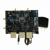
Manufacturer Part Number
AD6655-150EBZ
Description
BOARD EVAL FOR 150MSPS AD6655
Manufacturer
Analog Devices Inc
Type
Receiverr
Datasheet
1.AD6655-125EBZ.pdf
(88 pages)
Specifications of AD6655-150EBZ
Frequency
0Hz ~ 450MHz
Silicon Manufacturer
Analog Devices
Application Sub Type
IF Diversity Receiver
Kit Application Type
Communication & Networking
Silicon Core Number
AD6655
Kit Contents
Evaluation Board With AD6655 And Software
Lead Free Status / RoHS Status
Lead free / RoHS Compliant
For Use With/related Products
AD6655
Lead Free Status / RoHS Status
Lead free / RoHS Compliant, Lead free / RoHS Compliant


MEMORY
In addition, the first input sample signal power is updated in
the accumulator, and the accumulation continues with the
subsequent input samples. Figure 77 illustrates the rms
magnitude monitoring logic.
For rms magnitude mode, the value in the signal monitor result
(SMR) register is a 20-bit fixed-point number. The following
equation can be used to determine the rms magnitude in dBFS
from the MAG value in the register. Note that if the signal
monitor period (SMP) is a power of 2, the second term in the
equation becomes 0.
For ms magnitude mode, the value in the SMR is a 20-bit fixed-
point number. The following equation can be used to determine
the ms magnitude in dBFS from the MAG value in the register.
Note that if the SMP is a power of 2, the second term in the
equation becomes 0.
THRESHOLD CROSSING MODE
In the threshold crossing mode of operation, the magnitude of
the input port signal is monitored over a programmable time
period (given by SMPR) to count the number of times it crosses
a certain programmable threshold value. This mode is set by
programming Logic 1x (where x is a don’t care bit) in the signal
monitor mode bits of the signal monitor control register or by
setting the threshold crossing output enable bit in the signal
monitor SPORT control register. Before activating this mode,
the user needs to program the 24-bit SMPR and the 13-bit
upper threshold register for each individual input port. The
same upper threshold register is used for both signal monitor-
ing and gain control (see the ADC Overrange and Gain Control
section).
After entering this mode, the value in the SMPR is loaded into a
monitor period timer, and the countdown is started. The
magnitude of the input signal is compared with the upper
threshold register (programmed previously) on each input clock
cycle. If the input signal has a magnitude greater than the upper
threshold register, the internal count register is incremented by 1.
The initial value of the internal count register is set to 0. This
comparison and incrementing of the internal count register
continues until the monitor period timer reaches a count of 1.
PORTS
FROM
FROM
INPUT
MAP
RMS Magnitude = 20 log
MS Magnitude = 10 log
Figure 77. ADC Input RMS Magnitude Monitoring Block Diagram
PERIOD REGISTER
POWER MONITOR
ACCUMULATOR
CLEAR
LOAD
COUNTER
DOWN
⎛
⎜
⎝
⎛
⎜
⎝
MAG
2
MAG
20
2
20
POWER MONITOR
⎞
⎟
⎠
LOAD
⎞
⎟
⎠
−
IS COUNT = 1?
REGISTER
HOLDING
−
10
10
log
log
⎡
⎢ ⎣
2
⎡
⎢ ⎣
ceil
2
ceil
CONTROLLER
SMP
[
log
INTERRUPT
MEMORY
[
SMP
log
2
MAP
TO
(
2
SMP
TO
(
SMP
)
]
)
⎤
⎥ ⎦
]
Rev. A | Page 45 of 88
⎤
⎥ ⎦
When the monitor period timer reaches a count of 1, the value
in the internal count register is transferred to the signal monitor
holding register, which can be read through the SPI port or
output through the SPORT serial port.
The monitor period timer is reloaded with the value in the
SMPR register, and the countdown is restarted. The internal
count register is also cleared to a value of 0. Figure 78 illustrates
the threshold crossing logic. The value in the SMR register is
the number of samples that have a magnitude greater than the
threshold register.
MEMORY
MEMORY
ADDITIONAL CONTROL BITS
For additional flexibility in the signal monitoring process, two
control bits are provided in the signal monitor control register.
They are the signal monitor enable bit and the complex power
calculation mode enable bit.
Signal Monitor Enable Bit
The signal monitor enable bit, located in Bit 0 of Register 0x112,
enables operation of the signal monitor block. If the signal
monitor function is not needed in a particular application, this
bit should be cleared to conserve power.
Complex Power Calculation Mode Enable Bit
When this bit is set, the part assumes that Channel A is digitizing
the I data and Channel B is digitizing the Q data for a complex
input signal (or vice versa). In this mode, the power reported is
equal to
This result is presented in the Signal Monitor DC Value Channel A
register if the signal monitor mode bits are set to 00. The Signal
Monitor DC Value Channel B register continues to compute the
Channel B value.
DC CORRECTION
Because the dc offset of the ADC may be significantly larger
than the signal being measured, a dc correction circuit is included
to null the dc offset before measuring the power. The dc correction
circuit can also be switched into the main signal path, but this
may not be appropriate if the ADC is digitizing a time-varying
signal with significant dc content, such as GSM.
PORTS
FROM
FROM
INPUT
FROM
MAP
MAP
THRESHOLD
I +
PERIOD REGISTER
POWER MONITOR
REGISTER
2
Figure 78. ADC Input Threshold Crossing Block Diagram
UPPER
Q
A
2
COMPARE
A>B
B
LOAD
CLEAR
COUNTER
DOWN
COMPARE
A>B
IS COUNT = 1?
POWER MONITOR
LOAD
REGISTER
HOLDING
CONTROLLER
INTERRUPT
AD6655
TO
MEMORY
MAP
TO
Related parts for AD6655-150EBZ
Image
Part Number
Description
Manufacturer
Datasheet
Request
R

Part Number:
Description:
BOARD EVAL W/AD6655 & SOFTWARE
Manufacturer:
Analog Devices Inc
Datasheet:

Part Number:
Description:
±1.7g Dual-Axis IMEMS Accelerometer Evaluation Board
Manufacturer:
Analog Devices Inc
Datasheet:

Part Number:
Description:
Inertial Sensor Evaluation System
Manufacturer:
Analog Devices Inc
Datasheet:
Part Number:
Description:
Manufacturer:
Analog Devices Inc
Datasheet:
Part Number:
Description:
Manufacturer:
Analog Devices Inc
Datasheet:
Part Number:
Description:
Manufacturer:
Analog Devices Inc
Datasheet:
Part Number:
Description:
Manufacturer:
Analog Devices Inc
Datasheet:
Part Number:
Description:
Manufacturer:
Analog Devices Inc
Datasheet:
Part Number:
Description:
Manufacturer:
Analog Devices Inc
Datasheet:
Part Number:
Description:
Manufacturer:
Analog Devices Inc
Datasheet:
Part Number:
Description:
Manufacturer:
Analog Devices Inc
Datasheet:
Part Number:
Description:
Manufacturer:
Analog Devices Inc
Datasheet:
Part Number:
Description:
Manufacturer:
Analog Devices Inc
Datasheet: