RMPA0959 Fairchild Semiconductor, RMPA0959 Datasheet - Page 11
RMPA0959
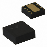
Manufacturer Part Number
RMPA0959
Description
IC MOD RF POWER AMP 10PIN 4X4LCC
Manufacturer
Fairchild Semiconductor
Type
Power Amplifierr
Specifications of RMPA0959
Current - Supply
62mA
Frequency
824MHz ~ 849MHz
Gain
25dB ~ 26.5dB
Noise Figure
4dB
Package / Case
11-LCC
Rf Type
Cellular, CDMA, CDMA2000, AMPS, IS-95
Voltage - Supply
3V ~ 4.2V
Number Of Channels
1
Frequency (max)
849MHz
Output Power
28dBm
Power Supply Requirement
Dual
Single Supply Voltage (min)
Not RequiredV
Single Supply Voltage (typ)
Not RequiredV
Single Supply Voltage (max)
Not RequiredV
Package Type
PLCC
Dual Supply Voltage (min)
3V
Dual Supply Voltage (typ)
3.4V
Dual Supply Voltage (max)
4.2V
Operating Temperature Classification
Commercial
Operating Temp Range
-30C to 85C
Pin Count
10
Mounting
Surface Mount
Lead Free Status / RoHS Status
Lead free / RoHS Compliant
P1db
-
Test Frequency
-
Lead Free Status / Rohs Status
Compliant
Other names
RMPA0959TR
Available stocks
Company
Part Number
Manufacturer
Quantity
Price
Company:

Part Number:
RMPA0959
Manufacturer:
FAI
Quantity:
4 498
Company:
Part Number:
RMPA0959-108
Manufacturer:
VISHAY
Quantity:
500


RMPA0959 Rev. F
Application Information
CAUTION: THIS IS AN ESD SENSITIVE DEVICE
Precautions
Damage:
• Cleanliness: Observe proper handling procedures
• Device
• Static Sensitivity: Follow ESD precautions to
• General Handling: Handle the package on the top
• Device Storage: Devices are supplied in heat-
Device Usage:
Fairchild recommends the following procedures prior
to assembly.
• Dry-bake devices at 125°C for 24 hours minimum.
• Assemble the dry-baked devices within 7 days of
• During the 7-day period, the devices must be
• If the 7-day period or the environmental conditions
to ensure clean devices and PCBs. Devices
should remain in their original packaging until
component placement to ensure no contamination
or damage to RF, DC & ground contact areas.
techniques should not present device problems
provided that the boards are properly dried to
remove solvents or water residues.
protect against ESD damage:
– A properly grounded static-dissipative surface
– Static-dissipative floor or mat.
– A properly grounded conductive wrist strap for
with a vacuum collet or along the edges with a
sharp pair of bent tweezers. Avoiding damaging
the RF, DC, & ground contacts on the package
bottom. Do not apply excessive pressure to the top
of the lid.
sealed, moisture-barrier bags. In this condition,
devices are protected and require no special
storage conditions. Once the sealed bag has been
opened, devices should be stored in a dry nitrogen
environment.
Note: The shipping trays cannot withstand 125°C
baking temperature.
removal from the oven.
stored in an environment of less than 60% relative
humidity and a maximum temperature of 30°C
have been exceeded, then the dry-bake procedure
must be repeated.
on which to place devices.
each person to wear while handling devices.
Cleaning:
to
Avoid
Standard
Permanent
board
cleaning
Device
11
Solder Materials & Temperature Profile: Reflow
soldering
attachment. Hand soldering is not recommended.
• Reflow Profile
Solder Joint Characteristics:
Proper operation of this device depends on a reliable
void-free attachment of the heatsink to the PWB. The
solder joint should be 95% void-free and be a
consistent thickness.
Rework Considerations:
Rework of a device attached to a board is limited to
reflow of the solder with a heat gun. The device
should not be subjected to more than 225°C and
reflow solder in the molten state for more than 5
seconds. No more than 2 rework operations should
be performed.
– Ramp-up: During this stage the solvents are
– Pre-heat/soak: The soak temperature stage
– Reflow Zone: If the temperature is too high, then
– Cooling Zone: Steep thermal gradients may give
evaporated from the solder paste. Care should
be taken to prevent rapid oxidation (or paste
slump) and solder bursts caused by violent
solvent out-gassing. A typical heating rate is 1-
2°C/sec.
serves two purposes; the flux is activated and
the board and devices achieve a uniform
temperature. The recommended soak condition
is: 120-150 seconds at 150°C.
devices may be damaged by mechanical stress
due to thermal mismatch or there may be
problems due to excessive solder oxidation.
Excessive time at temperature can enhance the
formation of inter-metallic compounds at the
lead/board interface and may lead to early
mechanical failure of the joint. Reflow must
occur prior to the flux being completely driven
off. The duration of peak reflow temperature
should not exceed 10 seconds. Maximum
soldering temperatures should be in the range
215-220°C, with a maximum limit of 225°C.
rise to excessive thermal shock. However, rapid
cooling promotes a finer grain structure and a
more crack-resistant solder joint. The illustration
below indicates the recommended soldering
profile.
is
the
preferred
method
of
www.fairchildsemi.com
SMT
Related parts for RMPA0959
Image
Part Number
Description
Manufacturer
Datasheet
Request
R

Part Number:
Description:
Fairchild Semiconductor [IGBT MODULE]
Manufacturer:
Fairchild Semiconductor
Datasheet:

Part Number:
Description:
Discrete Semiconductor Modules
Manufacturer:
Fairchild Semiconductor
Part Number:
Description:
Discrete Semiconductor Modules
Manufacturer:
Fairchild Semiconductor
Part Number:
Description:
This N-Channel MOSFET is produced using Fairchild Semiconductor’s advanced Power Trench® process
Manufacturer:
Fairchild Semiconductor
Datasheet:
Part Number:
Description:
This N-Channel MOSFET is produced using Fairchild Semiconductor’s advanced Power Trench® process
Manufacturer:
Fairchild Semiconductor
Datasheet:
Part Number:
Description:
This N-Channel MOSFET is produced using Fairchild Semiconductor’s advanced PowerTrench® process
Manufacturer:
Fairchild Semiconductor
Datasheet:
Part Number:
Description:
This N-Channel MOSFET is produced using Fairchild Semiconductor’s advanced PowerTrench® process
Manufacturer:
Fairchild Semiconductor
Datasheet:
Part Number:
Description:
This N-Channel MOSFET is produced using Fairchild Semiconductor’s advanced Power Trench® process
Manufacturer:
Fairchild Semiconductor
Datasheet:
Part Number:
Description:
This N-Channel logic Level MOSFETs are produced using Fairchild Semiconductor‘s advanced Power Trench® process that has been special tailored to minimize the on-state resistance and yet maintain superior switching performance
Manufacturer:
Fairchild Semiconductor
Datasheet:
Part Number:
Description:
This N-Channel MOSFET is produced using Fairchild Semiconductor’s advanced Power Trench® process
Manufacturer:
Fairchild Semiconductor
Datasheet:
Part Number:
Description:
This N-Channel SyncFET™ is produced using Fairchild Semiconductor’s advanced PowerTrench® process
Manufacturer:
Fairchild Semiconductor
Datasheet:
Part Number:
Description:
This N-Channel SyncFET™ is produced using Fairchild Semiconductor’s advanced PowerTrench® process
Manufacturer:
Fairchild Semiconductor
Datasheet:
Part Number:
Description:
This N-Channel SyncFET™ is produced using Fairchild Semiconductor’s advanced PowerTrench® process
Manufacturer:
Fairchild Semiconductor
Datasheet:
Part Number:
Description:
This N-Channel logic Level MOSFETs are produced using Fairchild Semiconductor‘s advanced Power Trench® process that has been special tailored to minimize the on-state resistance and yet maintain superior switching performance
Manufacturer:
Fairchild Semiconductor
Datasheet:
Part Number:
Description:
This N-Channel MOSFET is produced using Fairchild Semiconductor’s advanced Power Trench® process that has been especially tailored to minimize the on-state resistance and yet maintain superior switching performance
Manufacturer:
Fairchild Semiconductor
Datasheet: