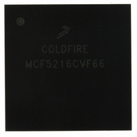
MCF5216CVF66 Freescale Semiconductor, MCF5216CVF66 Datasheet - Page 668

MCF5216CVF66
Manufacturer Part Number
MCF5216CVF66
Description
IC MPU 32BIT COLDF 256-MAPBGA
Manufacturer
Freescale Semiconductor
Series
MCF521xr
Datasheet
1.MCF5216CVM66J.pdf
(766 pages)
Specifications of MCF5216CVF66
Core Processor
Coldfire V2
Core Size
32-Bit
Speed
66MHz
Connectivity
CAN, EBI/EMI, I²C, SPI, UART/USART
Peripherals
DMA, LVD, POR, PWM, WDT
Number Of I /o
142
Program Memory Size
512KB (512K x 8)
Program Memory Type
FLASH
Ram Size
64K x 8
Voltage - Supply (vcc/vdd)
2.7 V ~ 3.6 V
Data Converters
A/D 8x12b
Oscillator Type
Internal
Operating Temperature
-40°C ~ 85°C
Package / Case
256-MAPBGA
Controller Family/series
ColdFire
Ram Memory Size
64KB
Embedded Interface Type
CAN, I2C, SPI, UART
No. Of Pwm Channels
8
Operating Temperature Range
-40°C To +85°C
No. Of Pins
256
Rohs Compliant
No
Package
256MA-BGA
Device Core
ColdFire
Family Name
MCF521x
Maximum Speed
66 MHz
Operating Supply Voltage
3.3 V
Data Bus Width
32 Bit
Number Of Programmable I/os
142
Interface Type
QSPI/UART/I2C/CAN
On-chip Adc
8-chx10-bit
Number Of Timers
8
Lead Free Status / RoHS Status
Contains lead / RoHS non-compliant
Eeprom Size
-
Available stocks
Company
Part Number
Manufacturer
Quantity
Price
Company:
Part Number:
MCF5216CVF66
Manufacturer:
FSC
Quantity:
1 670
Company:
Part Number:
MCF5216CVF66
Manufacturer:
Freescale Semiconductor
Quantity:
10 000
Part Number:
MCF5216CVF66
Manufacturer:
FREESCALE
Quantity:
20 000
Company:
Part Number:
MCF5216CVF66J
Manufacturer:
Freescale Semiconductor
Quantity:
10 000
- Current page: 668 of 766
- Download datasheet (9Mb)
IEEE 1149.1 Test Access Port (JTAG)
The DSCLK pin clocks the serial communication port to the debug module. Maximum frequency is 1/5
the processor clock speed. At the rising edge of DSCLK, the data input on DSI is sampled and DSO
changes state.
31.3.1.6 TDO/DSO — Test Data Output / Development Serial Output
The TDO pin is the LSB-first data output. Data is clocked out of TDO on the falling edge of TCLK. TDO
is tri-stateable and is actively driven in the shift-IR and shift-DR controller states.
The DSO pin provides serial output data in BDM mode.
31.4
31.4.1
The JTAG module registers are not memory mapped and are only accessible through the TDO/DSO pin.
31.4.2
All registers are shift-in and parallel load.
31.4.2.1 Instruction Shift Register (IR)
The JTAG module uses a 4-bit shift register with no parity. The IR transfers its value to a parallel hold
register and applies an instruction on the falling edge of TCLK when the TAP state machine is in the
update-IR state. To load an instruction into the shift portion of the IR, place the serial data on the TDI pin
before each rising edge of TCLK. The MSB of the IR is the bit closest to the TDI pin, and the LSB is the
bit closest to the TDO pin.
31.4.2.2 IDCODE Register
The IDCODE is a read-only register; its value is chip dependent. For more information, see
Section 31.5.3.2, “IDCODE
31-4
Reset PRN[3] PRN[2] PRN[1] PRN[0]
Reset
Field
Field
R/W
R/W
31
15
Memory Map/Register Definition
Memory Map
Register Descriptions
PRN[[3:0]
PIN[9:0]
MCF5282 and MCF5216 ColdFire Microcontroller User’s Manual, Rev. 3
Instruction.”
28
12
27
11
Figure 31-2. IDCODE Register
0000_0000_0000_0000
0111_01
DC[5:0]
Read only
Read only
JEDEC[10]
22
PIN[9] PIN[8] PIN[7] PIN[6] PIN[5] PIN[4]
21
PIN[9:0]
Freescale Semiconductor
1
ID
16
0
Related parts for MCF5216CVF66
Image
Part Number
Description
Manufacturer
Datasheet
Request
R
Part Number:
Description:
Manufacturer:
Freescale Semiconductor, Inc
Datasheet:
Part Number:
Description:
Manufacturer:
Freescale Semiconductor, Inc
Datasheet:
Part Number:
Description:
Manufacturer:
Freescale Semiconductor, Inc
Datasheet:
Part Number:
Description:
Manufacturer:
Freescale Semiconductor, Inc
Datasheet:
Part Number:
Description:
Manufacturer:
Freescale Semiconductor, Inc
Datasheet:
Part Number:
Description:
Manufacturer:
Freescale Semiconductor, Inc
Datasheet:
Part Number:
Description:
Manufacturer:
Freescale Semiconductor, Inc
Datasheet:
Part Number:
Description:
Manufacturer:
Freescale Semiconductor, Inc
Datasheet:
Part Number:
Description:
Manufacturer:
Freescale Semiconductor, Inc
Datasheet:
Part Number:
Description:
Manufacturer:
Freescale Semiconductor, Inc
Datasheet:
Part Number:
Description:
Manufacturer:
Freescale Semiconductor, Inc
Datasheet:
Part Number:
Description:
Manufacturer:
Freescale Semiconductor, Inc
Datasheet:
Part Number:
Description:
Manufacturer:
Freescale Semiconductor, Inc
Datasheet:
Part Number:
Description:
Manufacturer:
Freescale Semiconductor, Inc
Datasheet:
Part Number:
Description:
Manufacturer:
Freescale Semiconductor, Inc
Datasheet:


