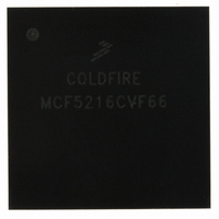
MCF5216CVF66 Freescale Semiconductor, MCF5216CVF66 Datasheet - Page 117

MCF5216CVF66
Manufacturer Part Number
MCF5216CVF66
Description
IC MPU 32BIT COLDF 256-MAPBGA
Manufacturer
Freescale Semiconductor
Series
MCF521xr
Datasheet
1.MCF5216CVM66J.pdf
(766 pages)
Specifications of MCF5216CVF66
Core Processor
Coldfire V2
Core Size
32-Bit
Speed
66MHz
Connectivity
CAN, EBI/EMI, I²C, SPI, UART/USART
Peripherals
DMA, LVD, POR, PWM, WDT
Number Of I /o
142
Program Memory Size
512KB (512K x 8)
Program Memory Type
FLASH
Ram Size
64K x 8
Voltage - Supply (vcc/vdd)
2.7 V ~ 3.6 V
Data Converters
A/D 8x12b
Oscillator Type
Internal
Operating Temperature
-40°C ~ 85°C
Package / Case
256-MAPBGA
Controller Family/series
ColdFire
Ram Memory Size
64KB
Embedded Interface Type
CAN, I2C, SPI, UART
No. Of Pwm Channels
8
Operating Temperature Range
-40°C To +85°C
No. Of Pins
256
Rohs Compliant
No
Package
256MA-BGA
Device Core
ColdFire
Family Name
MCF521x
Maximum Speed
66 MHz
Operating Supply Voltage
3.3 V
Data Bus Width
32 Bit
Number Of Programmable I/os
142
Interface Type
QSPI/UART/I2C/CAN
On-chip Adc
8-chx10-bit
Number Of Timers
8
Lead Free Status / RoHS Status
Contains lead / RoHS non-compliant
Eeprom Size
-
Available stocks
Company
Part Number
Manufacturer
Quantity
Price
Company:
Part Number:
MCF5216CVF66
Manufacturer:
FSC
Quantity:
1 670
Company:
Part Number:
MCF5216CVF66
Manufacturer:
Freescale Semiconductor
Quantity:
10 000
Part Number:
MCF5216CVF66
Manufacturer:
FREESCALE
Quantity:
20 000
Company:
Part Number:
MCF5216CVF66J
Manufacturer:
Freescale Semiconductor
Quantity:
10 000
- Current page: 117 of 766
- Download datasheet (9Mb)
6.3.1
The CFM configuration field comprises 24 bytes of reserved array memory space that determines the
module protection and access restrictions out of reset. Data to secure the Flash from unauthorized access
is also stored in the CFM configuration field.
6.3.2
The configuration information in the Flash base address register (FLASHBAR) controls the operation of
the Flash module.
The FLASHBAR register contains several control fields. These fields are shown in
Freescale Semiconductor
•
•
•
•
•
0x0000_040C–0x0000_040F
0x0000_0408–0x0000_040B
Address Offset (from array
0x0000_0400–0x0000_0407
0x0000_0410–0x0000_0413
0x0000_0414–0x0000_0417
The FLASHBAR holds the base address of the Flash. The MOVEC instruction provides write-only
access to this register.
The FLASHBAR can be read or written from the debug module in a similar manner.
All undefined bits in the register are reserved. These bits are ignored during writes to the
FLASHBAR, and return zeroes when read from the debug module.
The back door enable bit, FLASHBAR[BDE], is cleared at reset, disabling back door access to the
Flash.
The FLASHBAR valid bit is programmed according to the chip mode selected at reset (see
Chapter 27, “Chip Configuration Module
base address)
CFM Configuration Field
Flash Base Address Register (FLASHBAR)
The default value of the FLASHBAR is determined by the chip
configuration selected at reset (see
Module
the FLASHBAR located in the processor’s CPU space will be invalid and it
must be initialized with the valid bit set before the CPU (or modules) can
access the on-chip Flash.
(CCM)” for more information). If external boot mode is used, then
MCF5282 and MCF5216 ColdFire Microcontroller User’s Manual, Rev. 3
in Bytes
Size
Table 6-1. CFM Configuration Field
8
4
4
4
4
Back door comparison key
Flash program/erase sector protection
Blocks 0H/0L (see
(CFMPROT)”)
Flash supervisor/user space restrictions
Blocks 0H/0L (see
(CFMSACC)”)
Flash program/data space restrictions
Blocks 0H/0L (see
(CFMDACC)”)
Flash security longword (see
(CFMSEC)”)
Table 6-1
NOTE
(CCM)” for more details). All other bits are unaffected.
Chapter 27, “Chip Configuration
describes each byte used in this field.
Section 6.3.4.4, “CFM Protection Register
Section 6.3.4.5, “CFM Supervisor Access Register
Section 6.3.4.6, “CFM Data Access Register
Description
Section 6.3.4.3, “CFM Security Register
ColdFire Flash Module (CFM)
Figure 6-3
6-5
Related parts for MCF5216CVF66
Image
Part Number
Description
Manufacturer
Datasheet
Request
R
Part Number:
Description:
Manufacturer:
Freescale Semiconductor, Inc
Datasheet:
Part Number:
Description:
Manufacturer:
Freescale Semiconductor, Inc
Datasheet:
Part Number:
Description:
Manufacturer:
Freescale Semiconductor, Inc
Datasheet:
Part Number:
Description:
Manufacturer:
Freescale Semiconductor, Inc
Datasheet:
Part Number:
Description:
Manufacturer:
Freescale Semiconductor, Inc
Datasheet:
Part Number:
Description:
Manufacturer:
Freescale Semiconductor, Inc
Datasheet:
Part Number:
Description:
Manufacturer:
Freescale Semiconductor, Inc
Datasheet:
Part Number:
Description:
Manufacturer:
Freescale Semiconductor, Inc
Datasheet:
Part Number:
Description:
Manufacturer:
Freescale Semiconductor, Inc
Datasheet:
Part Number:
Description:
Manufacturer:
Freescale Semiconductor, Inc
Datasheet:
Part Number:
Description:
Manufacturer:
Freescale Semiconductor, Inc
Datasheet:
Part Number:
Description:
Manufacturer:
Freescale Semiconductor, Inc
Datasheet:
Part Number:
Description:
Manufacturer:
Freescale Semiconductor, Inc
Datasheet:
Part Number:
Description:
Manufacturer:
Freescale Semiconductor, Inc
Datasheet:
Part Number:
Description:
Manufacturer:
Freescale Semiconductor, Inc
Datasheet:


