ADM1062ASUZ Analog Devices Inc, ADM1062ASUZ Datasheet - Page 5
ADM1062ASUZ
Manufacturer Part Number
ADM1062ASUZ
Description
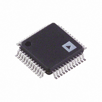
IC SUPERVISOR/SEQUENCER 48-TQFP
Manufacturer
Analog Devices Inc
Type
Sequencerr
Datasheet
1.EVAL-ADM1062LFEB.pdf
(36 pages)
Specifications of ADM1062ASUZ
Number Of Voltages Monitored
10
Output
Programmable
Voltage - Threshold
Adjustable/Selectable
Operating Temperature
-40°C ~ 85°C
Mounting Type
Surface Mount
Package / Case
48-TQFP, 48-VQFP
For Use With
EVAL-ADM1062TQEBZ - BOARD EVALUATION FOR ADM1062TQEVAL-ADM1062LFEBZ - BOARD EVALUATION FOR ADM1062LF
Lead Free Status / RoHS Status
Lead free / RoHS Compliant
Reset
-
Reset Timeout
-
Available stocks
Company
Part Number
Manufacturer
Quantity
Price
Company:

Part Number:
ADM1062ASUZ
Manufacturer:
Analog Devices Inc
Quantity:
10 000
Part Number:
ADM1062ASUZ
Manufacturer:
ADI/亚德诺
Quantity:
20 000
Company:
Part Number:
ADM1062ASUZ-REEL7
Manufacturer:
Analog Devices Inc
Quantity:
10 000


Parameter
TEMPERATURE SENSOR
BUFFERED VOLTAGE OUTPUT DACs
REFERENCE OUTPUT
PROGRAMMABLE DRIVER OUTPUTS (PDOs)
Conversion Time
Offset Error
Input Noise
Local Sensor Accuracy
Local Sensor Supply Voltage Coefficient
Remote Sensor Accuracy
Remote Sensor Supply Voltage Coefficient
Remote Sensor Current Source
Temperature for Code 0x800
Temperature for Code 0xC00
Temperature Resolution per Code
Resolution
Code 0x80 Output Voltage
Output Voltage Range
LSB Step Size
INL
DNL
Gain Error
Maximum Load Current (Source)
Maximum Load Current (Sink)
Maximum Load Capacitance
Settling Time to 50 pF Load
Load Regulation
PSRR
Reference Output Voltage
Load Regulation
Minimum Load Capacitance
PSRR
High Voltage (Charge Pump) Mode
Standard (Digital Output) Mode
Range 1
Range 2
Range 3
Range 4
(PDO1 to PDO6)
Output Impedance
V
I
(PDO1 to PDO10)
V
V
OUTAVG
OH
OH
OL
2
Min
0.592
0.796
0.996
1.246
2.043
1
11
10.5
2.4
V
0
PU
− 0.3
Typ
0.44
84
0.25
±3
−1.7
±3
−3
200
12
0
128
0.125
8
0.6
0.8
1
1.25
601.25
2.36
100
100
2.5
60
40
2.048
−0.25
+0.25
60
500
12.5
12
20
Rev. B | Page 5 of 36
Max
±2
0.603
0.803
1.003
1.253
±0.75
±0.4
1
50
2
2.053
14
13.5
4.5
0.50
Unit
ms
ms
LSB
LSB rms
°C
°C/V
°C
°C
μA
μA
°C
°C
°C
Bits
V
V
V
V
mV
mV
LSB
LSB
%
μA
μA
pF
μs
mV
dB
dB
V
mV
mV
μF
dB
kΩ
V
V
μA
V
V
V
V
Low level
Same range, independent of center point
Test Conditions/Comments
One conversion on one channel
All 12 channels selected, 16× averaging enabled
V
Direct input (no attenuator)
VDDCAP = 4.75 V
VDDCAP = 4.75 V
High level
VDDCAP = 4.75 V
VDDCAP = 4.75 V
Six DACs are individually selectable for centering on
one of four output voltage ranges
Endpoint corrected
Per mA
DC
100 mV step in 20 ns with 50 pF load
No load
Sourcing current, I
Sinking current, I
Capacitor required for decoupling, stability
DC
I
I
2 V < V
V
V
V
I
OH
OH
OL
REFIN
PU
PU
PU
= 20 mA
= 0 μA
= 1 μA
(pull-up to VDDCAP or VPx) = 2.7 V, I
to VPx = 6.0 V, I
≤ 2.7 V, I
= 2.048 V
OH
< 7 V
OH
= 0.5 mA
DACxMAX
DACxMAX
OH
= 0 mA
= +100 μA
= −100 μA
OH
ADM1062
= 0.5 mA
Related parts for ADM1062ASUZ
Image
Part Number
Description
Manufacturer
Datasheet
Request
R


Part Number:
Description:
±1.7g Dual-Axis IMEMS Accelerometer Evaluation Board
Manufacturer:
Analog Devices Inc
Datasheet:

Part Number:
Description:
Inertial Sensor Evaluation System
Manufacturer:
Analog Devices Inc
Datasheet:
Part Number:
Description:
Manufacturer:
Analog Devices Inc
Datasheet:
Part Number:
Description:
Manufacturer:
Analog Devices Inc
Datasheet:
Part Number:
Description:
Manufacturer:
Analog Devices Inc
Datasheet:
Part Number:
Description:
Manufacturer:
Analog Devices Inc
Datasheet:
Part Number:
Description:
Manufacturer:
Analog Devices Inc
Datasheet:
Part Number:
Description:
Manufacturer:
Analog Devices Inc
Datasheet:
Part Number:
Description:
Manufacturer:
Analog Devices Inc
Datasheet:
Part Number:
Description:
Manufacturer:
Analog Devices Inc
Datasheet:
Part Number:
Description:
Manufacturer:
Analog Devices Inc
Datasheet:
Part Number:
Description:
Manufacturer:
Analog Devices Inc
Datasheet: