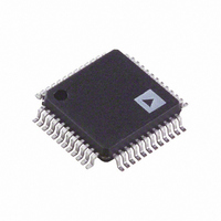
ADM1062ASUZ Analog Devices Inc, ADM1062ASUZ Datasheet - Page 15

ADM1062ASUZ
Manufacturer Part Number
ADM1062ASUZ
Description
IC SUPERVISOR/SEQUENCER 48-TQFP
Manufacturer
Analog Devices Inc
Type
Sequencerr
Datasheet
1.EVAL-ADM1062LFEB.pdf
(36 pages)
Specifications of ADM1062ASUZ
Number Of Voltages Monitored
10
Output
Programmable
Voltage - Threshold
Adjustable/Selectable
Operating Temperature
-40°C ~ 85°C
Mounting Type
Surface Mount
Package / Case
48-TQFP, 48-VQFP
For Use With
EVAL-ADM1062TQEBZ - BOARD EVALUATION FOR ADM1062TQEVAL-ADM1062LFEBZ - BOARD EVALUATION FOR ADM1062LF
Lead Free Status / RoHS Status
Lead free / RoHS Compliant
Reset
-
Reset Timeout
-
Available stocks
Company
Part Number
Manufacturer
Quantity
Price
Company:
Part Number:
ADM1062ASUZ
Manufacturer:
Analog Devices Inc
Quantity:
10 000
Part Number:
ADM1062ASUZ
Manufacturer:
ADI/亚德诺
Quantity:
20 000
Company:
Part Number:
ADM1062ASUZ-REEL7
Manufacturer:
Analog Devices Inc
Quantity:
10 000
The hysteresis value is given by
where:
V
N
Note that N
hysteresis for the ranges is listed in Table 6.
INPUT GLITCH FILTERING
The final stage of the SFDs is a glitch filter. This block provides
time-domain filtering on the output of the SFD comparators,
which allows the user to remove any spurious transitions, such
as supply bounce at turn-on. The glitch filter function is in addition
to the digitally programmable hysteresis of the SFD comparators.
The glitch filter timeout is programmable up to 100 μs.
For example, when the glitch filter timeout is 100 μs, any pulse
appearing on the input of the glitch filter block that is less than
100 μs in duration is prevented from appearing on the output of
the glitch filter block. Any input pulse that is longer than 100 μs
appears on the output of the glitch filter block. The output is
delayed with respect to the input by 100 μs. The filtering
process is shown in Figure 23.
SUPPLY SUPERVISION WITH VXx INPUTS
The VXx inputs have two functions. They can be used as either
supply fault detectors or digital logic inputs. When selected as
analog (SFD) inputs, the VXx pins have functionality that is
very similar to the VH and VPx pins. The primary difference is
that the VXx pins have only one input range: 0.573 V to 1.375 V.
Therefore, these inputs can directly supervise only the very low
supplies. However, the input impedance of the VXx pins is high,
allowing an external resistor divide network to be connected to the
pin. Thus, potentially any supply can be divided down into the
input range of the VXx pin and supervised, enabling the ADM1062
to monitor other supplies, such as +24 V, +48 V, and −5 V.
HYST
THRESH
t
t
PROGRAMMED
0
0
THAN GLITCH FILTER TIMEOUT
INPUT
V
TIMEOUT
is the desired hysteresis voltage.
INPUT PULSE SHORTER
HYST
is the decimal value of the 5-bit hysteresis code.
= V
THRESH
t
t
R
GF
GF
× N
OUTPUT
Figure 23. Input Glitch Filter Function
has a maximum value of 31. The maximum
THRESH
/255
PROGRAMMED
THAN GLITCH FILTER TIMEOUT
t
t
0
0
TIMEOUT
INPUT PULSE LONGER
INPUT
t
t
GF
GF
OUTPUT
Rev. B | Page 15 of 36
An additional supply supervision function is available when the
VXx pins are selected as digital inputs. In this case, the analog
function is available as a second detector on each of the dedi-
cated analog inputs, VPx and VH. The analog function of VX1
is mapped to VP1, VX2 is mapped to VP2, and so on; VX5 is
mapped to VH. In this case, these SFDs can be viewed as secondary
or warning SFDs.
The secondary SFDs are fixed to the same input range as the
primary SFDs. They are used to indicate warning levels rather
than failure levels. This allows faults and warnings to be gener-
ated on a single supply using only one pin. For example, if VP1
is set to output a fault when a 3.3 V supply drops to 3.0 V, VX1
can be set to output a warning at 3.1 V. Warning outputs are
available for readback from the status registers. They are also
OR’ e d together and fed into the SE, allowing warnings to generate
interrupts on the PDOs. Therefore, in this example, if the
supply drops to 3.1 V, a warning is generated and remedial
action can be taken before the supply drops out of tolerance.
VXx PINS AS DIGITAL INPUTS
As discussed in the Supply Supervision with VXX Inputs section,
the VXx input pins on the ADM1062 have dual functionality. The
second function is as a digital logic input to the device. Therefore,
the ADM1062 can be configured for up to five digital inputs. These
inputs are TTL-/CMOS-compatible. Standard logic signals can
be applied to the pins: RESET from reset generators, PWRGD
signals, fault flags, manual resets, and so on. These signals are
available as inputs to the SE and, therefore, can be used to control
the status of the PDOs. The inputs can be configured to detect
either a change in level or an edge.
When configured for level detection, the output of the digital
block is a buffered version of the input. When configured for
edge detection, a pulse of programmable width is output from
the digital block once the logic transition is detected. The width
is programmable from 0 μs to 100 μs.
The digital blocks feature the same glitch filter function that is
available on the SFDs. This function enables the user to ignore
spurious transitions on the inputs. For example, the filter can be
used to debounce a manual reset switch.
When configured as digital inputs, each VXx pin has a weak
(10 μA) pull-down current source available for placing the input
into a known condition, even if left floating. The current source,
if selected, weakly pulls the input to GND.
(DIGITAL INPUT)
VXx
VREF = 1.4V
Figure 24. VXx Digital Input Function
+
–
DETECTOR
GLITCH
FILTER
ADM1062
TO
SEQUENCING
ENGINE


