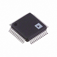
ADM1062ASUZ Analog Devices Inc, ADM1062ASUZ Datasheet - Page 31

ADM1062ASUZ
Manufacturer Part Number
ADM1062ASUZ
Description
IC SUPERVISOR/SEQUENCER 48-TQFP
Manufacturer
Analog Devices Inc
Type
Sequencerr
Datasheet
1.EVAL-ADM1062LFEB.pdf
(36 pages)
Specifications of ADM1062ASUZ
Number Of Voltages Monitored
10
Output
Programmable
Voltage - Threshold
Adjustable/Selectable
Operating Temperature
-40°C ~ 85°C
Mounting Type
Surface Mount
Package / Case
48-TQFP, 48-VQFP
For Use With
EVAL-ADM1062TQEBZ - BOARD EVALUATION FOR ADM1062TQEVAL-ADM1062LFEBZ - BOARD EVALUATION FOR ADM1062LF
Lead Free Status / RoHS Status
Lead free / RoHS Compliant
Reset
-
Reset Timeout
-
Available stocks
Company
Part Number
Manufacturer
Quantity
Price
Company:
Part Number:
ADM1062ASUZ
Manufacturer:
Analog Devices Inc
Quantity:
10 000
Part Number:
ADM1062ASUZ
Manufacturer:
ADI/亚德诺
Quantity:
20 000
Company:
Part Number:
ADM1062ASUZ-REEL7
Manufacturer:
Analog Devices Inc
Quantity:
10 000
•
•
Block Write
In a block write operation, the master device writes a block of
data to a slave device. The start address for a block write must
have been set previously. In the ADM1062, a send byte opera-
tion sets a RAM address, and a write byte/word operation sets
an EEPROM address, as follows:
1.
2.
3.
4.
5.
6.
S
1
To set up a 2-byte EEPROM address for a subsequent read,
write, block read, block write, or page erase. In this case, the
command byte is the high byte of EEPROM Address 0xF8
to EEPROM Address 0xFB. The only data byte is the low
byte of the EEPROM address, as shown in Figure 45.
To write a single byte of data to the EEPROM. In this case,
the command byte is the high byte of EEPROM Address 0xF8
to EEPROM Address 0xFB. The first data byte is the low
byte of the EEPROM address, and the second data byte is
the actual data, as shown in Figure 46.
The master device asserts a start condition on SDA.
The master sends the 7-bit slave address followed by
the write bit (low).
The addressed slave device asserts an ACK on SDA.
The master sends a command code that tells the slave
device to expect a block write. The ADM1062 command
code for a block write is 0xFC (1111 1100).
The slave asserts an ACK on SDA.
The master sends a data byte that tells the slave device how
many data bytes are being sent. The SMBus specification
allows a maximum of 32 data bytes in a block write.
Because a page consists of 32 bytes, only the three MSBs
of the address low byte are important for page erasure. The
lower five bits of the EEPROM address low byte specify the
addresses within a page and are ignored during an erase
operation.
ADDRESS
SLAVE
S
1
ADDRESS
2
SLAVE
2
Figure 46. Single Byte Write to the EEPROM
W A
Figure 45. Setting an EEPROM Address
3
W A
(0xF8 TO 0xFB)
3
HIGH BYTE
ADDRESS
EEPROM
(0xF8 TO 0xFB)
HIGH BYTE
ADDRESS
4
EEPROM
4
5
A
(0x00 TO 0xFF)
A
5
LOW BYTE
ADDRESS
EEPROM
(0x00 TO 0xFF)
6
LOW BYTE
ADDRESS
EEPROM
6
A
7
DATA
8
A
7
8
P
A
9
10
P
Rev. B | Page 31 of 36
7.
8.
9.
10. The master asserts a stop condition on SDA to end the
Unlike some EEPROM devices that limit block writes to within
a page boundary, there is no limitation on the start address
when performing a block write to EEPROM, except when
•
•
Note that the ADM1062 features a clock extend function for
writes to EEPROM. Programming an EEPROM byte takes
approximately 250 μs, which limits the SMBus clock for repeated
or block write operations. The ADM1062 pulls SCL low and
extends the clock pulse when it cannot accept any more data.
READ OPERATIONS
The ADM1062 uses the following SMBus read protocols.
Receive Byte
In a receive byte operation, the master device receives a single
byte from a slave device, as follows:
1.
2.
3.
4.
5.
6.
In the ADM1062, the receive byte protocol is used to read a
single byte of data from a RAM or EEPROM location whose
address has previously been set by a send byte or write
byte/word operation, as shown in Figure 48.
S
1
ADDRESS
SLAVE
The slave asserts an ACK on SDA.
The master sends N data bytes.
The slave asserts an ACK on SDA after each data byte.
transaction.
There must be at least N locations from the start address to
the highest EEPROM address (0xFBFF) to avoid writing to
invalid addresses.
An address crosses a page boundary. In this case, both
pages must be erased before programming.
The master device asserts a start condition on SDA.
The master sends the 7-bit slave address followed by the
read bit (high).
The addressed slave device asserts an ACK on SDA.
The master receives a data byte.
The master asserts a NACK on SDA.
The master asserts a stop condition on SDA, and the
transaction ends.
2
Figure 48. Single Byte Read from the EEPROM or RAM
W A
S
Figure 47. Block Write to the EEPROM or RAM
1
3
COMMAND 0xFC
(BLOCK WRITE)
ADDRESS
SLAVE
2
4
A
5
R
COUNT
BYTE
A
3
6
DATA
A
7
4
DATA
8
1
9
A
A
5
DATA
2
P
6
ADM1062
A
DATA
N
A P
10


