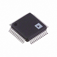
ADM1062ASUZ Analog Devices Inc, ADM1062ASUZ Datasheet - Page 4
ADM1062ASUZ
Manufacturer Part Number
ADM1062ASUZ
Description
IC SUPERVISOR/SEQUENCER 48-TQFP
Manufacturer
Analog Devices Inc
Type
Sequencerr
Datasheet
1.EVAL-ADM1062LFEB.pdf
(36 pages)
Specifications of ADM1062ASUZ
Number Of Voltages Monitored
10
Output
Programmable
Voltage - Threshold
Adjustable/Selectable
Operating Temperature
-40°C ~ 85°C
Mounting Type
Surface Mount
Package / Case
48-TQFP, 48-VQFP
For Use With
EVAL-ADM1062TQEBZ - BOARD EVALUATION FOR ADM1062TQEVAL-ADM1062LFEBZ - BOARD EVALUATION FOR ADM1062LF
Lead Free Status / RoHS Status
Lead free / RoHS Compliant
Reset
-
Reset Timeout
-
Available stocks
Company
Part Number
Manufacturer
Quantity
Price
Company:

Part Number:
ADM1062ASUZ
Manufacturer:
Analog Devices Inc
Quantity:
10 000
Part Number:
ADM1062ASUZ
Manufacturer:
ADI/亚德诺
Quantity:
20 000
Company:
Part Number:
ADM1062ASUZ-REEL7
Manufacturer:
Analog Devices Inc
Quantity:
10 000


ADM1062
SPECIFICATIONS
VH = 3.0 V to 14.4 V
Table 1.
Parameter
POWER SUPPLY ARBITRATION
POWER SUPPLY
SUPPLY FAULT DETECTORS
ANALOG-TO-DIGITAL CONVERTER
VH, VPx
VPx
VH
VDDCAP
C
Supply Current, I
Additional Currents
DAC Supply Currents
ADC Supply Current
EEPROM Erase Current
VH Pin
VPx Pins
VXx Pins
Absolute Accuracy
Threshold Resolution
Digital Glitch Filter
Signal Range
Input Reference Voltage on REFIN Pin, V
Resolution
INL
Gain Error
VDDCAP
All PDO FET Drivers On
Current Available from VDDCAP
Input Impedance
Input Attenuator Error
Detection Ranges
Input Impedance
Input Attenuator Error
Detection Ranges
Input Impedance
Detection Range
High Range
Midrange
Midrange
Low Range
Ultralow Range
Ultralow Range
VH
, I
1
VPx
, VPx = 3.0 V to 6.0 V
REFIN
1
, T
Min
3.0
2.7
10
6
2.5
2.5
1.25
0.573
1
0.573
0
A
= −40°C to +85°C, unless otherwise noted.
Typ
4.75
4.2
1
2.2
1
10
52
±0.05
52
±0.05
8
0
100
2.048
12
Rev. B | Page 4 of 36
Max
6.0
14.4
5.4
6
2
14.4
6
6
3
1.375
1.375
±1
V
±2.5
±0.05
REFIN
Unit
V
V
V
V
μF
mA
mA
mA
mA
mA
mA
kΩ
%
V
kΩ
%
V
V
MΩ
V
%
Bits
μs
μs
V
V
Bits
%
V
V
LSB
Test Conditions/Comments
Minimum supply required on one of the VH, VPx pins
Maximum VDDCAP = 5.1 V, typical
VDDCAP = 4.75 V
Regulated LDO output
Minimum recommended decoupling capacitance
VDDCAP = 4.75 V, PDO1 to PDO10 off, DACs off, ADC off
VDDCAP = 4.75 V, PDO1 to PDO6 loaded with 1 μA each,
PDO7 to PDO10 off
Maximum additional load that can be drawn from all
PDO pull-ups to VDDCAP
Six DACs on with 100 μA maximum load on each
Running round-robin loop
1 ms duration only, VDDCAP = 3 V
Midrange and high range
Low range and midrange
No input attenuation error
No input attenuation error
VREF error + DAC nonlinearity + comparator offset error +
input attenuation error
Minimum programmable filter length
Maximum programmable filter length
The ADC can convert signals presented to the VH, VPx,
and VXx pins; VPx and VH input signals are attenuated
depending on the selected range; a signal at the pin
corresponding to the selected range is from 0.573 V to
1.375 V at the ADC input
Endpoint corrected, V
V
REFIN
= 2.048 V
REFIN
= 2.048 V
Related parts for ADM1062ASUZ
Image
Part Number
Description
Manufacturer
Datasheet
Request
R


Part Number:
Description:
±1.7g Dual-Axis IMEMS Accelerometer Evaluation Board
Manufacturer:
Analog Devices Inc
Datasheet:

Part Number:
Description:
Inertial Sensor Evaluation System
Manufacturer:
Analog Devices Inc
Datasheet:
Part Number:
Description:
Manufacturer:
Analog Devices Inc
Datasheet:
Part Number:
Description:
Manufacturer:
Analog Devices Inc
Datasheet:
Part Number:
Description:
Manufacturer:
Analog Devices Inc
Datasheet:
Part Number:
Description:
Manufacturer:
Analog Devices Inc
Datasheet:
Part Number:
Description:
Manufacturer:
Analog Devices Inc
Datasheet:
Part Number:
Description:
Manufacturer:
Analog Devices Inc
Datasheet:
Part Number:
Description:
Manufacturer:
Analog Devices Inc
Datasheet:
Part Number:
Description:
Manufacturer:
Analog Devices Inc
Datasheet:
Part Number:
Description:
Manufacturer:
Analog Devices Inc
Datasheet:
Part Number:
Description:
Manufacturer:
Analog Devices Inc
Datasheet: