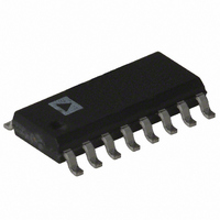
AD605ARZ Analog Devices Inc, AD605ARZ Datasheet - Page 8

AD605ARZ
Manufacturer Part Number
AD605ARZ
Description
IC AMP VGA DUAL LN 40MA 16SOIC
Manufacturer
Analog Devices Inc
Series
X-AMP®r
Type
Variable Gain Amplifierr
Datasheet
1.AD605-EVALZ.pdf
(24 pages)
Specifications of AD605ARZ
Amplifier Type
Variable Gain
Number Of Circuits
2
Slew Rate
170 V/µs
-3db Bandwidth
40MHz
Current - Input Bias
400nA
Current - Supply
18mA
Current - Output / Channel
40mA
Voltage - Supply, Single/dual (±)
4.5 V ~ 5.5 V
Operating Temperature
-40°C ~ 85°C
Mounting Type
Surface Mount
Package / Case
16-SOIC (3.9mm Width)
No. Of Amplifiers
1
Bandwidth
40MHz
Gain Accuracy
1.2dB
No. Of Channels
2
Supply Voltage Range
4.5V To 5.5V
Amplifier Case Style
SOIC
No. Of Pins
16
Number Of Channels
2
Number Of Elements
2
Power Supply Requirement
Single
Common Mode Rejection Ratio
20dB
Voltage Gain Db
34dB
Input Resistance
0.000175@5VMohm
Input Bias Current
0.4@5VnA
Single Supply Voltage (typ)
5V
Dual Supply Voltage (typ)
Not RequiredV
Power Dissipation
90W
Rail/rail I/o Type
No
Single Supply Voltage (min)
4.5V
Single Supply Voltage (max)
5.5V
Dual Supply Voltage (min)
Not RequiredV
Dual Supply Voltage (max)
Not RequiredV
Operating Temp Range
-40C to 85C
Operating Temperature Classification
Industrial
Mounting
Surface Mount
Pin Count
16
Package Type
SOIC N
Lead Free Status / RoHS Status
Lead free / RoHS Compliant
For Use With
AD605-EVALZ - BOARD EVALUATION FOR AD605
Output Type
-
Gain Bandwidth Product
-
Voltage - Input Offset
-
Lead Free Status / Rohs Status
Compliant
Available stocks
Company
Part Number
Manufacturer
Quantity
Price
Part Number:
AD605ARZ
Manufacturer:
ADI/亚德诺
Quantity:
20 000
Company:
Part Number:
AD605ARZ-RL
Manufacturer:
PANASONIC
Quantity:
20 000
AD605
–0.5
–1.0
–1.5
–2.0
20
18
16
14
12
10
2.0
1.5
1.0
0.5
20
18
16
14
12
10
8
6
4
2
0
8
6
4
2
0
0
Figure 9. Gain Error vs. VGN for Two Gain Scale Values
0.2
N = 50
ΔG(dB) = G(CH1) – G(CH2)
N = 50
ΔG(dB) = G(CH1) – G(CH2)
–0.8
–0.8
Figure 11. Gain Match, VGN1 = VGN2 = 2.50 V
Figure 10. Gain Match, VGN1 = VGN2 = 1.0 V
–0.6
–0.6
0.7
V
–0.4
REF
–0.4
30dB/V
= 1.67V
DELTA GAIN (dB)
DELTA GAIN (dB)
–0.2
–0.2
1.2
VGN (V)
0
0
1.7
0.2
0.2
0.4
0.4
V
REF
2.2
20dB/V
0.6
= 2.50V
0.6
0.8
0.8
2.7
Rev. F | Page 8 of 24
Figure 14. Output Referred Noise vs. VGN at Three Temperatures
2.525
2.520
2.515
2.510
2.505
2.500
2.495
2.490
2.485
2.480
2.475
–20
–40
–60
130
125
120
115
110
105
100
95
90
60
40
20
Figure 13. Output Offset vs. VGN at Three Temperatures
0
100k
0
0
V
Figure 12. AC Response for Three Values of VGN
OCM
VGN = 2.9V (FBK = OPEN)
VGN = 2.9V (FBK = SHORT)
VGN = 1.5V (FBK = OPEN)
VGN = 1.5V (FBK = SHORT)
VGN = 0.1V (FBK = OPEN)
VGN = 0.1V (FBK = SHORT)
= 2.50V
0.5
0.5
1.0
1.0
1M
FREQUENCY (Hz)
–40°C
+25°C
+85°C
VGN = 0.0V
VGN (V)
VGN (V)
1.5
1.5
+85°C
+25°C
–40°C
10M
2.0
2.0
2.5
2.5
100M
3.0
3.0


