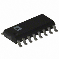
AD605ARZ Analog Devices Inc, AD605ARZ Datasheet - Page 18

AD605ARZ
Manufacturer Part Number
AD605ARZ
Description
IC AMP VGA DUAL LN 40MA 16SOIC
Manufacturer
Analog Devices Inc
Series
X-AMP®r
Type
Variable Gain Amplifierr
Datasheet
1.AD605-EVALZ.pdf
(24 pages)
Specifications of AD605ARZ
Amplifier Type
Variable Gain
Number Of Circuits
2
Slew Rate
170 V/µs
-3db Bandwidth
40MHz
Current - Input Bias
400nA
Current - Supply
18mA
Current - Output / Channel
40mA
Voltage - Supply, Single/dual (±)
4.5 V ~ 5.5 V
Operating Temperature
-40°C ~ 85°C
Mounting Type
Surface Mount
Package / Case
16-SOIC (3.9mm Width)
No. Of Amplifiers
1
Bandwidth
40MHz
Gain Accuracy
1.2dB
No. Of Channels
2
Supply Voltage Range
4.5V To 5.5V
Amplifier Case Style
SOIC
No. Of Pins
16
Number Of Channels
2
Number Of Elements
2
Power Supply Requirement
Single
Common Mode Rejection Ratio
20dB
Voltage Gain Db
34dB
Input Resistance
0.000175@5VMohm
Input Bias Current
0.4@5VnA
Single Supply Voltage (typ)
5V
Dual Supply Voltage (typ)
Not RequiredV
Power Dissipation
90W
Rail/rail I/o Type
No
Single Supply Voltage (min)
4.5V
Single Supply Voltage (max)
5.5V
Dual Supply Voltage (min)
Not RequiredV
Dual Supply Voltage (max)
Not RequiredV
Operating Temp Range
-40C to 85C
Operating Temperature Classification
Industrial
Mounting
Surface Mount
Pin Count
16
Package Type
SOIC N
Lead Free Status / RoHS Status
Lead free / RoHS Compliant
For Use With
AD605-EVALZ - BOARD EVALUATION FOR AD605
Output Type
-
Gain Bandwidth Product
-
Voltage - Input Offset
-
Lead Free Status / Rohs Status
Compliant
Available stocks
Company
Part Number
Manufacturer
Quantity
Price
Part Number:
AD605ARZ
Manufacturer:
ADI/亚德诺
Quantity:
20 000
Company:
Part Number:
AD605ARZ-RL
Manufacturer:
PANASONIC
Quantity:
20 000
AD605
EVALUATION BOARD
The AD605-EVALZ provides a platform for the circuit designer
to become familiar with the many operating and performance
features of the AD605 variable gain amplifier. It is a factory-
designed, surface-mount assembly fully tested and ready for
service. Figure 42 is a photograph of the AD605-EVALZ. Multiple
inputs, test points, and jumpers provide circuit configurations that
support any of the operating options of the device. Figure 43 is a
schematic of the board.
Power is required from only a single 5 V supply capable of
supplying 55 mA to 60 mA quiescent current.
Table 4. Table of Jumpers
Jumper
JP1
JP2
JP3
JP4
JP5
JP6
JP7
JP8
Function
Connects trimmer GN1ADJ to pin VGN1. This jumper can be removed for an ac signal at VGN1.
Grounds the IN1 pin via C2.
Grounds the IN2 pin via C5.
Connects trimmer GN2ADJ to Pin VGN2. This jumper can be removed for an ac signal at VGN2.
Connects trimmer VOCMADJ to the VOCM pin. This jumper can be removed for the half supply default VOCM.
Shifts the gain of Channel 2 up or down by 14 dB.
Shifts the gain of Channel 1 up or down by 14 dB.
Connects trimmer VREFADJ to the VREF pin to change the gain slope.
Figure 42. AD605–EVALZ Evaluation Board
Rev. F | Page 18 of 24
INPUT CONNECTIONS
The AD605 VGA accepts differential or single-ended input
signals and provides single-ended outputs. The SMA connectors
enable either configuration to be used, as well as the output and
gain control signals. Each of the I/O ports is also available at a
test-loop labeled for easy identification.
The input resistance at each of the four input SMA connectors is
50 Ω, consisting of the 175 Ω, ±40 Ω resistance of the attenuator
ladder network in parallel with the external 69.8 Ω resistors. For
single-ended operation, unused inputs can be left disconnected
or optional jumpers installed. Either VGA input is usable; for
noninverting operation, the INPx is used, and for signal inversion,
the INMx is used.
ADJUSTING GAIN, COMMON-MODE, AND
REFERENCE LEVELS
The gain of each channel is adjusted with trimmers, GN1ADJ and
GN2ADJ. Trimmer VREF ADJ adjusts the gain scaling in dB/V (or
gain slope), and VOCM ADJ adjusts the output common-mode
voltage for both channels. For dynamic gain control, JP1 and
JP4 can be removed and the signal applied at the SMA
connectors, GN1 and GN2.
OUTPUT CONNECTIONS
SMA connectors, OUT1 and OUT2, are the output connectors.
Series resistors and capacitors are included for termination and
dc blocking purposes. The output of the AD605 has a common-
mode value of one-half the supply (unless amended by a voltage
applied to the VCM pin).
Table 4 lists jumpers and their functions, and Figure 44 shows
the evaluation board in a typical test configuration.
Default Configuration
Installed
User supplied
User supplied
Installed
Installed
Installed
Installed
Installed


