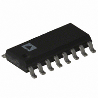
AD605ARZ Analog Devices Inc, AD605ARZ Datasheet - Page 15

AD605ARZ
Manufacturer Part Number
AD605ARZ
Description
IC AMP VGA DUAL LN 40MA 16SOIC
Manufacturer
Analog Devices Inc
Series
X-AMP®r
Type
Variable Gain Amplifierr
Datasheet
1.AD605-EVALZ.pdf
(24 pages)
Specifications of AD605ARZ
Amplifier Type
Variable Gain
Number Of Circuits
2
Slew Rate
170 V/µs
-3db Bandwidth
40MHz
Current - Input Bias
400nA
Current - Supply
18mA
Current - Output / Channel
40mA
Voltage - Supply, Single/dual (±)
4.5 V ~ 5.5 V
Operating Temperature
-40°C ~ 85°C
Mounting Type
Surface Mount
Package / Case
16-SOIC (3.9mm Width)
No. Of Amplifiers
1
Bandwidth
40MHz
Gain Accuracy
1.2dB
No. Of Channels
2
Supply Voltage Range
4.5V To 5.5V
Amplifier Case Style
SOIC
No. Of Pins
16
Number Of Channels
2
Number Of Elements
2
Power Supply Requirement
Single
Common Mode Rejection Ratio
20dB
Voltage Gain Db
34dB
Input Resistance
0.000175@5VMohm
Input Bias Current
0.4@5VnA
Single Supply Voltage (typ)
5V
Dual Supply Voltage (typ)
Not RequiredV
Power Dissipation
90W
Rail/rail I/o Type
No
Single Supply Voltage (min)
4.5V
Single Supply Voltage (max)
5.5V
Dual Supply Voltage (min)
Not RequiredV
Dual Supply Voltage (max)
Not RequiredV
Operating Temp Range
-40C to 85C
Operating Temperature Classification
Industrial
Mounting
Surface Mount
Pin Count
16
Package Type
SOIC N
Lead Free Status / RoHS Status
Lead free / RoHS Compliant
For Use With
AD605-EVALZ - BOARD EVALUATION FOR AD605
Output Type
-
Gain Bandwidth Product
-
Voltage - Input Offset
-
Lead Free Status / Rohs Status
Compliant
Available stocks
Company
Part Number
Manufacturer
Quantity
Price
Part Number:
AD605ARZ
Manufacturer:
ADI/亚德诺
Quantity:
20 000
Company:
Part Number:
AD605ARZ-RL
Manufacturer:
PANASONIC
Quantity:
20 000
Usable gain control voltage ranges are 0.1 V to 2.9 V for the
20 dB/V scale and 0.1 V to 1.45 V for the 40 dB/V scale. VGN
voltages of less than 0.1 V are not used for gain control because
below 50 mV the channel is powered down. This can be used to
conserve power and at the same time gate-off the signal. The
supply current for a powered-down channel is 1.9 mA, and the
response time to power the device on or off is less than 1 μs.
FIXED GAIN AMPLIFIER AND INTERPOLATOR
CIRCUITS—APPLYING AN ACTIVE FEEDBACK
AMPLIFIER
A typical X-amp architecture is powered by a dual polarity
power supply. Because the AD605 operates from a single supply, a
supply common equal to half the value of the supply voltage is
required. An active feedback amplifier (AFA) is used to provide
a differential input and to implement the feedback loop. The
AFA in the AD605 is an op amp with two g
in the feedback path, and the other is used as a highly linear
differential input.
A multisection distributed g
ladder network, one stage for each of the ladder nodes. Only a
few of the stages are active at any time and are dependent on the
gain control voltage.
–10
–15
–20
35
30
25
20
15
10
–5
5
0
0.5
Figure 37. Ideal Gain Curves vs. V
GAIN CONTROL VOLTAGE
1.0
40dB/V
m
stage senses the voltages on the
1.5
30dB/V
2.0
LINEAR-IN-dB RANGE
m
REF
stages; one is used
OF AD605
20dB/V
2.5
3.0
Rev. F | Page 15 of 24
The AFA makes a differential input structure possible because
one of its inputs (G1) is fully differential; this input is made
up of a distributed g
feedback. The output of G1 is some function of the voltages
sensed on the attenuator taps that is applied to a high gain
amplifier (A0). Because of negative feedback, the differential
input to the high gain amplifier is zero; this in turn implies that
the differential input voltage to G2 times g
of G2) is equal to the differential input voltage to G1 times g
(the transconductance of G1). Therefore, the overall gain
function of the AFA is
where:
V
V
( R1 + R2 )/ R2 = 42.
g
The AFA has additional features that include the following:
inverting the output signal by switching the positive and negative
input to the ladder network; the possibility of using the −IN
input as a second signal input; and independent control of the
DSX common-mode voltage. Under normal operating conditions,
it is best to connect a decoupling capacitor to Pin VOCM, in
which case, the common- mode voltage of the DSX is half of
the supply voltage; this allows for maximum signal swing.
Nevertheless, the common-mode voltage can be shifted up or
down by directly applying a voltage to VOCM. It can also be
used as another signal input, the only limitation being the
rather low slew rate of the VOCM buffer.
If the dc level of the output signal is not critical, another coupling
capacitor is normally used at the output of the DSX; again, this
is done for level shifting and to eliminate any dc offsets contributed
by the DSX (see the AC Coupling section).
The gain range of the DSX is programmable by a resistor connected
between Pin FBK and Pin OUT. The possible ranges are −14 dB to
+34.4 dB when the pins are shorted together or 0 dB to +48.4 dB
when FBK is left open. For the higher gain range, the bandwidth
of the amplifier is reduced by a factor of five to about 8 MHz
because the gain increased by 14 dB. This is the case for any
constant gain bandwidth product amplifier that includes the
active feedback amplifier.
m1
OUT
ATTEN
/ g
m2
is the output voltage.
V
V
is the effective voltage sensed on the attenuator.
ATTEN
= 1.25; the overall gain is therefore 52.5 (34.4 dB).
OUT
=
g
g
m
m
1
2
m
×
stage. The second input (G2) is used for
R1
R2
×
R2
m2
(the transconductance
AD605
m1
(7)


