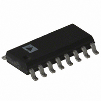
AD605ARZ Analog Devices Inc, AD605ARZ Datasheet

AD605ARZ
Specifications of AD605ARZ
Available stocks
Related parts for AD605ARZ
AD605ARZ Summary of contents
Page 1
FEATURES 2 independent linear-in-dB channels Input noise at maximum gain: 1.8 nV/√Hz, 2.7 pA/√Hz Bandwidth: 40 MHz (−3 dB) Differential input Absolute gain range programmable − +34 dB (FBK shorted to OUT) through ...
Page 2
AD605 TABLE OF CONTENTS Features .............................................................................................. 1 Applications ....................................................................................... 1 Functional Block Diagram .............................................................. 1 General Description ......................................................................... 1 Revision History ............................................................................... 2 Specifications ..................................................................................... 3 Absolute Maximum Ratings ............................................................ 5 ESD Caution .................................................................................. 5 Pin Configuration and Function Descriptions ...
Page 3
SPECIFICATIONS Each channel @ T = 25° unless otherwise noted. Table 1. Parameter Conditions INPUT CHARACTERISTICS Input Resistance Input Capacitance Peak Input Voltage At minimum gain Input Voltage Noise VGN = 2.9 ...
Page 4
AD605 Parameter Conditions GAIN CONTROL INTERFACE Gain Scaling Factor V REF V REF Gain Range FBK short to OUT FBK open Input Voltage (VGN) Range 20 dB/V, VREF = 2.5 V Input Bias Current Input Resistance Response Time 48 dB ...
Page 5
ABSOLUTE MAXIMUM RATINGS Table 2. Parameter Supply Voltage +V S Pin 12, Pin 13 (with Pin 4, Pin Input Voltage Pin 1 to Pin 3, Pin 6 to Pin 9, Pin 16 Internal Power Dissipation 16-Lead ...
Page 6
AD605 PIN CONFIGURATION AND FUNCTION DESCRIPTIONS Table 3. Pin Function Descriptions Pin No. Mnemonic Description 1 VGN1 CH1 Gain Control Input and Power-Down Pin. If grounded, device is off; otherwise, positive voltage increases gain. 2 −IN1 CH1 Negative Input. 3 ...
Page 7
TYPICAL PERFORMANCE CHARACTERISTICS (PER CHANNEL 2.5 V (20 dB/V scaling MHz, R REF 40 30 –40°C, +25°C, +85° –10 –20 0.1 0.5 0.9 1.3 1.7 VGN (V) Figure 3. Gain vs. VGN ...
Page 8
AD605 2.0 1.5 1.0 0.5 0 30dB/V –0 1.67V REF –1.0 –1.5 –2.0 0.2 0.7 1.2 1.7 VGN (V) Figure 9. Gain Error vs. VGN for Two Gain Scale Values ΔG(dB) = G(CH1) ...
Page 9
VGN (V) Figure 15. Input Referred Noise vs. VGN 2.00 VGN = 2.9V 1.95 1.90 1.85 1.80 1.75 1.70 1.65 1.60 –40 –30 –20 – ...
Page 10
AD605 – p-p –35 OUT VGN = 1.0V –40 –45 –50 –55 HD2 –60 –65 –70 100k 1M FREQUENCY (Hz) Figure 21. Harmonic Distortion vs. Frequency –35 –40 –45 HD2 –50 (1MHz) HD2 (10MHz) –55 –60 –65 ...
Page 11
TRIG'D –200 253ns 100ns/DIV Figure 27. Small Signal Pulse Response 500mV 2.9V 100 0.0V 500mV Figure 28. Power-Up/Power-Down Response 500mV 2.9V 100 0.1V 500mV Figure 29. Gain Response – 200mV p-p ...
Page 12
AD605 25 +I (AD605 (VGN = –40 –30 –20 – TEMPERATURE (°C) Figure 33. Supply Current (One Channel) vs. Temperature Rev. ...
Page 13
THEORY OF OPERATION The AD605 is a dual-channel, low noise VGA. Figure 35 shows the simplified block diagram of one channel. Each channel consists of a single-supply X-AMP® (hereafter called DSX, differential single-supply X-AMP) comprising the following: • Precision passive ...
Page 14
AD605 R –6.908dB R +IN 1.5R MID 1. –IN NOTE 96Ω 1.5R = 144Ω DIFFERENTIAL LADDER (ATTENUATOR) The attenuator before the fixed gain amplifier is realized by a differential, 7-stage, R-1.5R resistive ladder network with an ...
Page 15
GAIN CONTROL VOLTAGE –10 –15 –20 Figure 37. Ideal Gain Curves vs. V Usable gain control voltage ranges are 0 2.9 V for the ...
Page 16
AD605 APPLICATIONS INFORMATION The basic circuit in Figure 38 shows the connections for one channel of the AD605 with a gain range of − +34.4 dB. The signal is applied at +IN1. The ac coupling capacitors before Pin ...
Page 17
Figure 40 shows the gain vs. VGN for the circuit in Figure MHz and the lowest gain range (− +34.4 dB). Note that the gain scaling is 40 dB/V, double the 20 dB ...
Page 18
AD605 EVALUATION BOARD The AD605-EVALZ provides a platform for the circuit designer to become familiar with the many operating and performance features of the AD605 variable gain amplifier factory- designed, surface-mount assembly fully tested and ready for ...
Page 19
CH1_GN R1 DNI J1 GN1 VGA1_NEG J2 INM1 R4 69.8Ω JP2 VGA1_POS J3 INP1 R3 69.8Ω VGA2_POS J4 INP2 R6 69.8Ω VGA2_NEG J5 INM2 R5 JP3 69.8Ω CH2_GN J6 GN2 R7 DNI NOTES 1. PARTS IN GRAY ARE NOT INSTALLED. ...
Page 20
AD605 Figure 45. AD605-EVALZ Assembly Figure 46. AD605-EVALZ Primary Side Copper Figure 47. AD605-EVALZ Secondary Side Copper Figure 48. AD605-EVALZ Internal Ground Plane Figure 49. AD605-EVALZ Internal Power Plane Figure 50. AD605-EVALZ Primary Side Silkscreen Rev Page 20 ...
Page 21
OUTLINE DIMENSIONS 0.210 (5.33) MAX 0.150 (3.81) 0.130 (3.30) 0.115 (2.92) 0.022 (0.56) 0.018 (0.46) 0.014 (0.36) CONTROLLING DIMENSIONS ARE IN INCHES; MILLIMETER DIMENSIONS (IN PARENTHESES) ARE ROUNDED-OFF INCH EQUIVALENTS FOR REFERENCE ONLY AND ARE NOT APPROPRIATE FOR USE IN ...
Page 22
... AD605AR-REEL7 −40°C to +85°C AD605ARZ 1 −40°C to +85°C 1 AD605ARZ-RL −40°C to +85°C 1 AD605ARZ-R7 −40°C to +85°C AD605BN −40°C to +85°C AD605BR −40°C to +85°C AD605BR-REEL −40°C to +85°C AD605BR-REEL7 −40°C to +85°C ...
Page 23
NOTES Rev Page AD605 ...
Page 24
AD605 NOTES ©1996–2008 Analog Devices, Inc. All rights reserved. Trademarks and registered trademarks are the property of their respective owners. D00541-0-6/08(F) Rev Page ...


