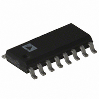
AD605ARZ Analog Devices Inc, AD605ARZ Datasheet - Page 13

AD605ARZ
Manufacturer Part Number
AD605ARZ
Description
IC AMP VGA DUAL LN 40MA 16SOIC
Manufacturer
Analog Devices Inc
Series
X-AMP®r
Type
Variable Gain Amplifierr
Datasheet
1.AD605-EVALZ.pdf
(24 pages)
Specifications of AD605ARZ
Amplifier Type
Variable Gain
Number Of Circuits
2
Slew Rate
170 V/µs
-3db Bandwidth
40MHz
Current - Input Bias
400nA
Current - Supply
18mA
Current - Output / Channel
40mA
Voltage - Supply, Single/dual (±)
4.5 V ~ 5.5 V
Operating Temperature
-40°C ~ 85°C
Mounting Type
Surface Mount
Package / Case
16-SOIC (3.9mm Width)
No. Of Amplifiers
1
Bandwidth
40MHz
Gain Accuracy
1.2dB
No. Of Channels
2
Supply Voltage Range
4.5V To 5.5V
Amplifier Case Style
SOIC
No. Of Pins
16
Number Of Channels
2
Number Of Elements
2
Power Supply Requirement
Single
Common Mode Rejection Ratio
20dB
Voltage Gain Db
34dB
Input Resistance
0.000175@5VMohm
Input Bias Current
0.4@5VnA
Single Supply Voltage (typ)
5V
Dual Supply Voltage (typ)
Not RequiredV
Power Dissipation
90W
Rail/rail I/o Type
No
Single Supply Voltage (min)
4.5V
Single Supply Voltage (max)
5.5V
Dual Supply Voltage (min)
Not RequiredV
Dual Supply Voltage (max)
Not RequiredV
Operating Temp Range
-40C to 85C
Operating Temperature Classification
Industrial
Mounting
Surface Mount
Pin Count
16
Package Type
SOIC N
Lead Free Status / RoHS Status
Lead free / RoHS Compliant
For Use With
AD605-EVALZ - BOARD EVALUATION FOR AD605
Output Type
-
Gain Bandwidth Product
-
Voltage - Input Offset
-
Lead Free Status / Rohs Status
Compliant
Available stocks
Company
Part Number
Manufacturer
Quantity
Price
Part Number:
AD605ARZ
Manufacturer:
ADI/亚德诺
Quantity:
20 000
Company:
Part Number:
AD605ARZ-RL
Manufacturer:
PANASONIC
Quantity:
20 000
THEORY OF OPERATION
The AD605 is a dual-channel, low noise VGA. Figure 35 shows
the simplified block diagram of one channel. Each channel consists
of a single-supply X-AMP® (hereafter called DSX, differential
single-supply X-AMP) comprising the following:
• Precision passive attenuator (differential ladder)
• Gain control block
• VOCM buffer with supply splitting resistors R3 and R4
• Active feedback amplifier
The linear-in-dB gain response of the AD605 can generally be
described by Equation 1.
where:
FB = 0, if FBK to OUT is shorted.
FB = 1, if FBK to OUT is open.
Each channel provides between −14 dB to +34.4 dB through
0 dB to +48.4 dB of gain, depending on the value of the resistance
connected between Pin FBK and Pin OUT. The center 40 dB of
gain is exactly linear-in-dB while the gain error increases at the top
and bottom of the range. The gain is set by the gain control voltage
(VGN). The VREF input establishes the gain scaling. The useful
gain scaling range is between 20 dB/V and 40 dB/V for a VREF
voltage of 2.5 V and 1.25 V, respectively. For example, if FBK to
OUT is shorted and VREF is set to 2.50 V (to establish a gain
scaling of 20 dB/V), the gain equation simplifies to
R1 and R2
G (dB) = (Gain Scaling (dB/V)) × (Gain Control (V)) −
(19 dB − (14 dB) × (FB))
G (dB) = (20 (dB/V)) × (VGN (V)) – 19 dB
VOCM
VREF
VGN
+IN
–IN
EXT
1
(AFA) with gain setting resistors
C3
VPOS
Figure 35. Simplified Block Diagram of a Single Channel of the AD605
R3
200kΩ
R4
200kΩ
C1
C2
+
EXT
Rev. F | Page 13 of 24
175Ω
175Ω
(1)
(2)
DIFFERENTIAL
ATTENUATOR
CONTROL
GAIN
The desired gain can then be achieved by setting the unipolar
gain control (VGN) to a voltage within its nominal operating
range of 0.25 V to 2.65 V (for 20 dB/V gain scaling). The gain is
monotonic for a complete gain control range of 0.1 V to 2.9 V.
Maximum gain can be achieved at a VGN of 2.9 V.
Because the two channels are identical, only Channel 1 is used
to describe their operation. VREF and VOCM are the only inputs
that are shared by the two channels, and because they are normally
ac grounds, crosstalk between the two channels is minimized.
For the highest gain scaling accuracy, VREF should have an
external low impedance voltage source. For low accuracy 20 dB/V
applications, the VREF input can be decoupled with a capacitor
to ground. In this mode, the gain scaling is determined by the
midpoint between +VCC and GND; therefore, care should be
taken to control the supply voltage to 5 V. The input resistance
looking into the VREF pin is 10 kΩ ± 20%.
The AD605 is a single-supply circuit, and the VOCM pin is used
to establish the dc level of the midpoint of this portion of the
circuit. VOCM needs only an external decoupling capacitor to
ground to center the midpoint between the supply voltages (5 V,
GND). However, if the dc level of the output is important to the
user (see the Applications Information section of the
data sheet for an example), VOCM can be specifically set. The
input resistance looking into the VOCM pin is 45 kΩ ± 20%.
1
20Ω
R2
To understand the active-feedback amplifier topology, refer to the
data sheet. The AD830 is a practical implementation of the idea.
+
+
G1
G2
DISTRIBUTED g
820Ω
R1
+
Ao
m
3.36kΩ
OUT
FBK
AD9050
AD605
AD830


