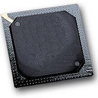
MPC5553MZQ132 Freescale Semiconductor, MPC5553MZQ132 Datasheet - Page 65

MPC5553MZQ132
Manufacturer Part Number
MPC5553MZQ132
Description
IC MCU MPC5553 REV A 324-PBGA
Manufacturer
Freescale Semiconductor
Series
MPC55xx Qorivvar
Datasheet
1.MPC5553EVBE.pdf
(68 pages)
Specifications of MPC5553MZQ132
Core Processor
e200z6
Core Size
32-Bit
Speed
132MHz
Connectivity
CAN, EBI/EMI, Ethernet, SCI, SPI
Peripherals
DMA, POR, PWM, WDT
Number Of I /o
220
Program Memory Size
1.5MB (1.5M x 8)
Program Memory Type
FLASH
Ram Size
64K x 8
Voltage - Supply (vcc/vdd)
1.35 V ~ 1.65 V
Data Converters
A/D 40x12b
Oscillator Type
External
Operating Temperature
-40°C ~ 125°C
Package / Case
324-PBGA
Processor Series
MPC5xxx
Core
e200z6
Data Bus Width
32 bit
Data Ram Size
64 KB
Interface Type
7-Wire, DSPI, ESCI
Maximum Clock Frequency
132 MHz
Number Of Timers
56
Maximum Operating Temperature
+ 125 C
Mounting Style
SMD/SMT
Minimum Operating Temperature
- 40 C
For Use With
MPC5553EVBISYS - KIT EVAL ISYSTEMS MPC5553MPC5553EVBGHS - KIT EVAL GREEN HILLS SOFTWAREMPC5553EVB - KIT EVAL MPC5553MZP132MPC5553EVBE - BOARD EVAL FOR MPC5553
Lead Free Status / RoHS Status
Lead free / RoHS Compliant
Eeprom Size
-
Lead Free Status / Rohs Status
No
Available stocks
Company
Part Number
Manufacturer
Quantity
Price
Company:
Part Number:
MPC5553MZQ132
Manufacturer:
Freescale Semiconductor
Quantity:
10 000
Freescale Semiconductor
Table 17
Table 19
Table 20
Table 21
Table 23
Table 24
Table 22
Location
Pad AC Specifications and
Reset and Configuration Pin Timing: Footnote 1, deleted ‘F
JTAG Pin AC Electrical Characteristics:
Nexus Debug Port Timing.
External Interrupt Timing:
eTPU Timing
Bus Operation Timing:
Footnote 1, deleted: ‘ and CL = 30 pF with DSC = 0b10, SRC = 0b11,’ changed ‘functional’ to ‘Nexus.’
Changed Spec 12, TCK Low to TDO Data Valid: Changed ‘VDDE = 3.0 to 3.6 volts’ maximum value in column 4
from 9 to 10. Now reads ‘V
•
• Footnote 1, deleted ‘F
• Footnote 2, changed from ‘tested’ to ‘(not tested).’
• Footnote 3, changed from ‘Out delay’ to ‘The output delay’,
• Changed from ‘Add a maximum of one system clock to the output delay to get the output delay with respect to
• Footnote 4: changed ‘Delay’ to ‘The output delay.’
• Footnote 5: deleted ‘before qualification.’ Changed from ‘This parameter is supplied for reference and is not
• Changed from ‘This parameter is supplied for reference and is not guaranteed by design and not tested’ to ‘This
• External Bus Frequency in the table heading: Added footnote that reads: Speed is the nominal maximum
• Spec 1: Changed the values in Min. columns: 40 MHz from 25 to 24.4; 56 MHz from 17.9 to 17.5
• Specs 7 and 8: Removed from external bus interface: BDIP, OE, WE/BE[0:1]; removed from the calibration bus
• Deleted duplicate footnote: The EBTS = 0 timings are tested and valid at V
• Added a footnote each for the DATA[0:31], TEA, and WE/BE[0:3] signals in the table: Due to pin limitations, the
• Footnote 1, changed ‘V
• Footnote 1: Deleted ‘F
• Deleted second figure after table ‘External Interrupt Setup Timing.’
• Footnote 1, changed ‘V
• Footnote 1: Deleted ‘F
• Deleted second figure, ‘eTPU Input/Output Timing’ after this table.
• Added Footnote 2: ‘This specification does not include the rise and fall times. When calculating the minimum
Table 17
the system clock‘ to ‘To calculate the output delay with respect to the system clock, add a maximum of one system
clock to the output delay.’
guaranteed by design and not tested’ to ‘This parameter is supplied for reference and is guaranteed by design
and tested.’
parameter is supplied for reference and is guaranteed by design and tested.’
frequency. Max speed is the maximum speed allowed including frequency modulation (FM). 82 MHz parts allow
for 80 MHz system clock + 2% FM;
114 MHz parts allow for 112 MHz system clock + 2% FM, and 132 MHz parts allow for 128 MHz system clock +
2% FM.
interface CAL_CS[0, 2:3], CAL_WE/BE[0:1].
EBTS = 1 timings are tested and valid at V
DATA[16:31], TEA, and WE/BE[2:3] signals are not available on the 324 package.
‘ and CL = 200 pF with SRC = 0b11.’
‘ and CL = 200 pF with SRC = 0b11.’
eTPU pulse width, include the rise and fall times defined in the slew rate control fields (SRC) of the pad
configuration registers (PCR).’
Table 33. Table and Figure Changes Between Rev. 2.0 and 3.0 (continued)
Pad AC Specifications ONLY: Footnote 1, changed ‘V
Table 18
SYS
SYS
SYS
DDEH
DDEH
MPC5553 Microcontroller Data Sheet, Rev. 3.0
DDE
= 132 MHz.’
= 132 MHz.’, ‘V
= 132 MHz.’, ‘V
= 3.0–3.6 V’ with a max value of 10.
= 4.5–5.5;’ to ‘V
= 4.5–5.5;’ to ‘V
Derated Pad AC Specifications: The changes are identical in the tables.
Description of Changes
DD
DD
DDE
DDEH
= 1.35–1.65 V’, ‘V
DDEH
= 1.35–1.65 V’,‘V
= 1.6–3.6 V.
= 4.5–5.25;’
= 4.5–5.25;’
SYS
= 132 MHz.’
DDEH
DD33
Revision History for the MPC5553 Data Sheet
DD33
and V
= 4.5–5.5;’ to ‘V
and V
DDSYN
DDSYN
DDE
= 2.25–3.6 V only, whereas
= 3.0–3.6’ and
= 3.0–3.6 V.’ and
DDEH
= 4.5–5.25;’
65


