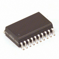
MC68HC908JB16JDW Freescale Semiconductor, MC68HC908JB16JDW Datasheet - Page 7
MC68HC908JB16JDW
Manufacturer Part Number
MC68HC908JB16JDW
Description
IC MCU 16K FLASH 6MHZ USB 20SOIC
Manufacturer
Freescale Semiconductor
Series
HC08r
Datasheet
1.MC908JB16DWE.pdf
(332 pages)
Specifications of MC68HC908JB16JDW
Core Processor
HC08
Core Size
8-Bit
Speed
6MHz
Connectivity
SCI, USB
Peripherals
LED, LVD, POR, PWM
Number Of I /o
13
Program Memory Size
16KB (16K x 8)
Program Memory Type
FLASH
Ram Size
384 x 8
Voltage - Supply (vcc/vdd)
4 V ~ 5.5 V
Oscillator Type
Internal
Operating Temperature
0°C ~ 70°C
Package / Case
20-SOIC (7.5mm Width)
Lead Free Status / RoHS Status
Contains lead / RoHS non-compliant
Eeprom Size
-
Data Converters
-
Available stocks
Company
Part Number
Manufacturer
Quantity
Price

Part Number:
MC68HC908JB16JDWE
Manufacturer:
FREESCALE
Quantity:
20 000


MC68HC908JB16
Freescale Semiconductor
Technical Data — MC68HC908JB16
—
Rev. 1.1
1.1
1.2
1.3
1.4
1.5
1.6
1.6.1
1.6.2
1.6.3
1.6.4
1.6.5
1.6.6
1.6.7
1.6.8
1.6.9
1.6.10
1.6.11
1.6.12
1.6.13
1.6.14
2.1
2.2
2.3
Contents . . . . . . . . . . . . . . . . . . . . . . . . . . . . . . . . . . . . . . . . . .29
Introduction . . . . . . . . . . . . . . . . . . . . . . . . . . . . . . . . . . . . . . . . 29
Features . . . . . . . . . . . . . . . . . . . . . . . . . . . . . . . . . . . . . . . . . . 30
MCU Block Diagram . . . . . . . . . . . . . . . . . . . . . . . . . . . . . . . . . 31
Pin Assignments . . . . . . . . . . . . . . . . . . . . . . . . . . . . . . . . . . . . 33
Pin Functions . . . . . . . . . . . . . . . . . . . . . . . . . . . . . . . . . . . . . .34
Contents . . . . . . . . . . . . . . . . . . . . . . . . . . . . . . . . . . . . . . . . . .41
Introduction . . . . . . . . . . . . . . . . . . . . . . . . . . . . . . . . . . . . . . . . 41
Unimplemented Memory Locations . . . . . . . . . . . . . . . . . . . . . 41
Power Supply Pins (V
Voltage Regulator Output Pin (V
Oscillator Pins (OSC1 and OSC2) . . . . . . . . . . . . . . . . . . . . 35
External Reset Pin (RST) . . . . . . . . . . . . . . . . . . . . . . . . . . . 35
External Interrupt Pins (IRQ, PTE4/D–) . . . . . . . . . . . . . . . . 35
CGM Power Supply Pins (V
CGM Voltage Regulator Out (V
CGM Voltage Regulator In (V
External Filter Capacitor Pins (CGMXFC1, CGMXFC2) . . . 36
CGM Clock Output Pins (CGMOUT1, CGMOUT2) . . . . . . . 36
Port A Input/Output (I/O) Pins (PTA7/KBA7–PTA0/KBA0). . 36
Port C I/O Pins (PTC1/RxD, PTC0/TxD) . . . . . . . . . . . . . . . 37
Port D I/O Pins (PTD5–PTD0) . . . . . . . . . . . . . . . . . . . . . . . 37
Port E I/O Pins (PTE4/D–, PTE3/D+, PTE2/T2CH01,
PTE1/T1CH01, PTE0/TCLK). . . . . . . . . . . . . . . . . . . . . . 37
Table of Contents
Section 1. General Description
Section 2. Memory Map
DD
, V
SS
DDA
REGA1
) . . . . . . . . . . . . . . . . . . . . . . . 34
REGA0
, V
Table of Contents
REG
SSA0
) . . . . . . . . . . . . . . . . . . 36
). . . . . . . . . . . . . . . . . . 34
) . . . . . . . . . . . . . . . . . 36
, V
SSA1
) . . . . . . . . . 36
Technical Data
7
Related parts for MC68HC908JB16JDW
Image
Part Number
Description
Manufacturer
Datasheet
Request
R

Part Number:
Description:
Manufacturer:
Freescale Semiconductor, Inc
Datasheet:
Part Number:
Description:
Manufacturer:
Freescale Semiconductor, Inc
Datasheet:
Part Number:
Description:
Manufacturer:
Freescale Semiconductor, Inc
Datasheet:
Part Number:
Description:
Manufacturer:
Freescale Semiconductor, Inc
Datasheet:
Part Number:
Description:
Manufacturer:
Freescale Semiconductor, Inc
Datasheet:
Part Number:
Description:
Manufacturer:
Freescale Semiconductor, Inc
Datasheet:
Part Number:
Description:
Manufacturer:
Freescale Semiconductor, Inc
Datasheet:
Part Number:
Description:
Manufacturer:
Freescale Semiconductor, Inc
Datasheet:
Part Number:
Description:
Manufacturer:
Freescale Semiconductor, Inc
Datasheet:
Part Number:
Description:
Manufacturer:
Freescale Semiconductor, Inc
Datasheet:
Part Number:
Description:
Manufacturer:
Freescale Semiconductor, Inc
Datasheet:
Part Number:
Description:
Manufacturer:
Freescale Semiconductor, Inc
Datasheet:
Part Number:
Description:
Manufacturer:
Freescale Semiconductor, Inc
Datasheet:
Part Number:
Description:
Manufacturer:
Freescale Semiconductor, Inc
Datasheet:
Part Number:
Description:
Manufacturer:
Freescale Semiconductor, Inc
Datasheet: