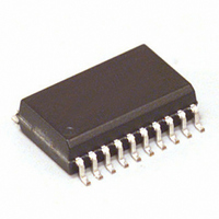
MC68HC908JB16JDW Freescale Semiconductor, MC68HC908JB16JDW Datasheet - Page 268

MC68HC908JB16JDW
Manufacturer Part Number
MC68HC908JB16JDW
Description
IC MCU 16K FLASH 6MHZ USB 20SOIC
Manufacturer
Freescale Semiconductor
Series
HC08r
Datasheet
1.MC908JB16DWE.pdf
(332 pages)
Specifications of MC68HC908JB16JDW
Core Processor
HC08
Core Size
8-Bit
Speed
6MHz
Connectivity
SCI, USB
Peripherals
LED, LVD, POR, PWM
Number Of I /o
13
Program Memory Size
16KB (16K x 8)
Program Memory Type
FLASH
Ram Size
384 x 8
Voltage - Supply (vcc/vdd)
4 V ~ 5.5 V
Oscillator Type
Internal
Operating Temperature
0°C ~ 70°C
Package / Case
20-SOIC (7.5mm Width)
Lead Free Status / RoHS Status
Contains lead / RoHS non-compliant
Eeprom Size
-
Data Converters
-
Available stocks
Company
Part Number
Manufacturer
Quantity
Price
Part Number:
MC68HC908JB16JDWE
Manufacturer:
FREESCALE
Quantity:
20 000
- Current page: 268 of 332
- Download datasheet (4Mb)
Input/Output (I/O) Ports
Technical Data
268
When bit DDRAx is a logic 1, reading address $0000 reads the PTAx
data latch. When bit DDRAx is a logic 0, reading address $0000 reads
the voltage level on the pin. The data latch can always be written,
regardless of the state of its data direction bit.
the operation of the port A pins.
Notes:
1. X = don’t care.
2. Hi-Z = high impedance.
3. Writing affects data register, but does not affect input.
DDRA
Bit
0
1
PTA Bit
Input/Output (I/O) Ports
X
X
(1)
Table 14-2. Port A Pin Functions
I/O Pin Mode
Input, Hi-Z
Output
(2)
Read/Write
DDRA[7:0]
DDRA[7:0]
Accesses
to DDRA
Table 14-2
MC68HC908JB16
PTA[7:0]
Freescale Semiconductor
Read
Accesses to PTA
Pin
summarizes
PTA[7:0]
PTA[7:0]
—
Write
Rev. 1.1
(3)
Related parts for MC68HC908JB16JDW
Image
Part Number
Description
Manufacturer
Datasheet
Request
R
Part Number:
Description:
Manufacturer:
Freescale Semiconductor, Inc
Datasheet:
Part Number:
Description:
Manufacturer:
Freescale Semiconductor, Inc
Datasheet:
Part Number:
Description:
Manufacturer:
Freescale Semiconductor, Inc
Datasheet:
Part Number:
Description:
Manufacturer:
Freescale Semiconductor, Inc
Datasheet:
Part Number:
Description:
Manufacturer:
Freescale Semiconductor, Inc
Datasheet:
Part Number:
Description:
Manufacturer:
Freescale Semiconductor, Inc
Datasheet:
Part Number:
Description:
Manufacturer:
Freescale Semiconductor, Inc
Datasheet:
Part Number:
Description:
Manufacturer:
Freescale Semiconductor, Inc
Datasheet:
Part Number:
Description:
Manufacturer:
Freescale Semiconductor, Inc
Datasheet:
Part Number:
Description:
Manufacturer:
Freescale Semiconductor, Inc
Datasheet:
Part Number:
Description:
Manufacturer:
Freescale Semiconductor, Inc
Datasheet:
Part Number:
Description:
Manufacturer:
Freescale Semiconductor, Inc
Datasheet:
Part Number:
Description:
Manufacturer:
Freescale Semiconductor, Inc
Datasheet:
Part Number:
Description:
Manufacturer:
Freescale Semiconductor, Inc
Datasheet:
Part Number:
Description:
Manufacturer:
Freescale Semiconductor, Inc
Datasheet:


