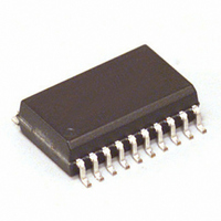
MC68HC908JB16JDW Freescale Semiconductor, MC68HC908JB16JDW Datasheet - Page 305

MC68HC908JB16JDW
Manufacturer Part Number
MC68HC908JB16JDW
Description
IC MCU 16K FLASH 6MHZ USB 20SOIC
Manufacturer
Freescale Semiconductor
Series
HC08r
Datasheet
1.MC908JB16DWE.pdf
(332 pages)
Specifications of MC68HC908JB16JDW
Core Processor
HC08
Core Size
8-Bit
Speed
6MHz
Connectivity
SCI, USB
Peripherals
LED, LVD, POR, PWM
Number Of I /o
13
Program Memory Size
16KB (16K x 8)
Program Memory Type
FLASH
Ram Size
384 x 8
Voltage - Supply (vcc/vdd)
4 V ~ 5.5 V
Oscillator Type
Internal
Operating Temperature
0°C ~ 70°C
Package / Case
20-SOIC (7.5mm Width)
Lead Free Status / RoHS Status
Contains lead / RoHS non-compliant
Eeprom Size
-
Data Converters
-
Available stocks
Company
Part Number
Manufacturer
Quantity
Price
Part Number:
MC68HC908JB16JDWE
Manufacturer:
FREESCALE
Quantity:
20 000
- Current page: 305 of 332
- Download datasheet (4Mb)
18.4.2 Low V
18.5 LVI Control and Configuration
MC68HC908JB16
Freescale Semiconductor
NOTE:
REG
—
Rev. 1.1
Detector
* LVIDR, LVI5OR3, URSTD, and LVID bits are reset by POR (power-on reset) or LVI reset only.
Address:
Reset:
The low V
LVI reset when the V
LVI circuit can be disabled by the setting the LVIDR bit in CONFIG.
There is no LVI circuit for V
Three bits in the configuration register (CONFIG) control the operation
of the LVI module.
LVIDR — LVI Disable Bit for V
LVI5OR3 — LVI Trip Point Voltage Select Bit for V
LVID — LVI Disable Bit for V
Read:
Write:
LVIDR disables the LVI circuit for V
LVI5OR3 selects the trip point voltage of the LVI circuit for V
Section 20. Electrical Specifications
LVID disables the LVI circuit for V
1 = LVI circuit for V
0 = LVI circuit for V
1 = LVI trips at 3.3V
0 = LVI trips at 2.4V
1 = LVI circuit for V
0 = LVI circuit for V
LVIDR
$001F
Bit 7
0*
Figure 18-2. Configuration Register (CONFIG)
REG
Low-Voltage Inhibit (LVI)
LVI5OR3
= Unimplemented
detector circuit monitors the V
0*
6
REG
URSTD
REG
REG
DD
DD
0*
5
voltage falls below the trip voltage. The V
REGA
disabled
enabled
DD
disabled
enabled
REG
LVID
.
0*
4
DD
REG
.
SSREC
for the trip voltage tolerances.
3
0
.
REG
COPRS
voltage and forces a
2
0
DD
Low-Voltage Inhibit (LVI)
STOP
1
0
Technical Data
DD
COPD
. See
Bit 0
REG
0
305
Related parts for MC68HC908JB16JDW
Image
Part Number
Description
Manufacturer
Datasheet
Request
R
Part Number:
Description:
Manufacturer:
Freescale Semiconductor, Inc
Datasheet:
Part Number:
Description:
Manufacturer:
Freescale Semiconductor, Inc
Datasheet:
Part Number:
Description:
Manufacturer:
Freescale Semiconductor, Inc
Datasheet:
Part Number:
Description:
Manufacturer:
Freescale Semiconductor, Inc
Datasheet:
Part Number:
Description:
Manufacturer:
Freescale Semiconductor, Inc
Datasheet:
Part Number:
Description:
Manufacturer:
Freescale Semiconductor, Inc
Datasheet:
Part Number:
Description:
Manufacturer:
Freescale Semiconductor, Inc
Datasheet:
Part Number:
Description:
Manufacturer:
Freescale Semiconductor, Inc
Datasheet:
Part Number:
Description:
Manufacturer:
Freescale Semiconductor, Inc
Datasheet:
Part Number:
Description:
Manufacturer:
Freescale Semiconductor, Inc
Datasheet:
Part Number:
Description:
Manufacturer:
Freescale Semiconductor, Inc
Datasheet:
Part Number:
Description:
Manufacturer:
Freescale Semiconductor, Inc
Datasheet:
Part Number:
Description:
Manufacturer:
Freescale Semiconductor, Inc
Datasheet:
Part Number:
Description:
Manufacturer:
Freescale Semiconductor, Inc
Datasheet:
Part Number:
Description:
Manufacturer:
Freescale Semiconductor, Inc
Datasheet:


