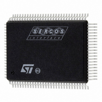
ST92F150JDV1QC STMicroelectronics, ST92F150JDV1QC Datasheet - Page 301

ST92F150JDV1QC
Manufacturer Part Number
ST92F150JDV1QC
Description
IC MCU 128K FLASH 100-PQFP
Manufacturer
STMicroelectronics
Series
ST9r
Datasheet
1.ST92F150CV1TB.pdf
(429 pages)
Specifications of ST92F150JDV1QC
Core Processor
ST9
Core Size
8/16-Bit
Speed
24MHz
Connectivity
CAN, I²C, LIN, SCI, SPI
Peripherals
DMA, LVD, POR, PWM, WDT
Number Of I /o
77
Program Memory Size
128KB (128K x 8)
Program Memory Type
FLASH
Eeprom Size
1K x 8
Ram Size
6K x 8
Voltage - Supply (vcc/vdd)
4.5 V ~ 5.5 V
Data Converters
A/D 16x10b
Oscillator Type
Internal
Operating Temperature
-40°C ~ 125°C
Package / Case
100-QFP
Processor Series
ST92F15x
Core
ST9
Data Bus Width
8 bit, 16 bit
Data Ram Size
6 KB
Interface Type
CAN, I2C, SCI, SPI
Maximum Clock Frequency
24 MHz
Number Of Programmable I/os
80
Number Of Timers
5 x 16 bit
Operating Supply Voltage
4.5 V to 5.5 V
Maximum Operating Temperature
+ 105 C
Mounting Style
SMD/SMT
Development Tools By Supplier
ST92F150-EPB
Minimum Operating Temperature
- 40 C
On-chip Adc
16 bit x 10 bit
Case
QFP
Lead Free Status / RoHS Status
Lead free / RoHS Compliant
Other names
497-2137
Available stocks
Company
Part Number
Manufacturer
Quantity
Price
- Current page: 301 of 429
- Download datasheet (8Mb)
J1850 BYTE LEVEL PROTOCOL DECODER (Cont’d)
10.9.6.3 DMA Management in Reception Mode
The DMA in reception is performed when the
RDRF bit of the STATUS register is set (by hard-
ware). The RDRF bit is reset as soon as the DMA
cycle is finished.
To enable the DMA feature, the RXD_M bit of the
IMR register must be set (by software).
Each DMA request performs the transfer of a sin-
gle byte from the RXDATA register of the peripher-
al toward Register File or Memory Space
139).
Each DMA transfer consists of three operations
that are performed with minimum use of CPU time:
– A load from the JBLPD data register (RXDATA)
Figure 139. DMA in Reception Mode
to a location of Register File/Memory addressed
JBLPD peripheral
RXDATA
(Figure
J1850 Byte Level Protocol Decoder (JBLPD)
– A post-increment of the DMA Address Register
– A post-decrement of the DMA transaction coun-
Note: When the REOBP pending bit is set (at the
end of the last DMA transfer), the reception DMA
enable bit (RXD_M) is automatically reset by hard-
ware. However, the DMA can be disabled by soft-
ware resetting the RXD_M bit.
Note: The DMA request acknowledge could de-
pend on the priority level stored in the PRLR regis-
ter.
through the DMA Address Register (or Register
pair);
(or Register pair);
ter, which contains the number of transactions
that have still to be performed.
Data received
Previous data
Memory space
Register File
Current
Address
Pointer
or
301/429
9
Related parts for ST92F150JDV1QC
Image
Part Number
Description
Manufacturer
Datasheet
Request
R

Part Number:
Description:
BOARD PROGRAM FOR ST92F150 MCU
Manufacturer:
STMicroelectronics
Datasheet:

Part Number:
Description:
BOARD EVALUATION FOR ST9 SERIES
Manufacturer:
STMicroelectronics
Datasheet:

Part Number:
Description:
BOARD EMULATOR FOR ST9 SERIES
Manufacturer:
STMicroelectronics
Datasheet:

Part Number:
Description:
MCU, MPU & DSP Development Tools ST9 Dedication Board
Manufacturer:
STMicroelectronics
Datasheet:

Part Number:
Description:
STMicroelectronics [RIPPLE-CARRY BINARY COUNTER/DIVIDERS]
Manufacturer:
STMicroelectronics
Datasheet:

Part Number:
Description:
STMicroelectronics [LIQUID-CRYSTAL DISPLAY DRIVERS]
Manufacturer:
STMicroelectronics
Datasheet:

Part Number:
Description:
BOARD EVAL FOR MEMS SENSORS
Manufacturer:
STMicroelectronics
Datasheet:

Part Number:
Description:
NPN TRANSISTOR POWER MODULE
Manufacturer:
STMicroelectronics
Datasheet:

Part Number:
Description:
TURBOSWITCH ULTRA-FAST HIGH VOLTAGE DIODE
Manufacturer:
STMicroelectronics
Datasheet:

Part Number:
Description:
Manufacturer:
STMicroelectronics
Datasheet:

Part Number:
Description:
DIODE / SCR MODULE
Manufacturer:
STMicroelectronics
Datasheet:

Part Number:
Description:
DIODE / SCR MODULE
Manufacturer:
STMicroelectronics
Datasheet:


