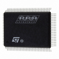
ST92F150JDV1QC STMicroelectronics, ST92F150JDV1QC Datasheet - Page 150

ST92F150JDV1QC
Manufacturer Part Number
ST92F150JDV1QC
Description
IC MCU 128K FLASH 100-PQFP
Manufacturer
STMicroelectronics
Series
ST9r
Datasheet
1.ST92F150CV1TB.pdf
(429 pages)
Specifications of ST92F150JDV1QC
Core Processor
ST9
Core Size
8/16-Bit
Speed
24MHz
Connectivity
CAN, I²C, LIN, SCI, SPI
Peripherals
DMA, LVD, POR, PWM, WDT
Number Of I /o
77
Program Memory Size
128KB (128K x 8)
Program Memory Type
FLASH
Eeprom Size
1K x 8
Ram Size
6K x 8
Voltage - Supply (vcc/vdd)
4.5 V ~ 5.5 V
Data Converters
A/D 16x10b
Oscillator Type
Internal
Operating Temperature
-40°C ~ 125°C
Package / Case
100-QFP
Processor Series
ST92F15x
Core
ST9
Data Bus Width
8 bit, 16 bit
Data Ram Size
6 KB
Interface Type
CAN, I2C, SCI, SPI
Maximum Clock Frequency
24 MHz
Number Of Programmable I/os
80
Number Of Timers
5 x 16 bit
Operating Supply Voltage
4.5 V to 5.5 V
Maximum Operating Temperature
+ 105 C
Mounting Style
SMD/SMT
Development Tools By Supplier
ST92F150-EPB
Minimum Operating Temperature
- 40 C
On-chip Adc
16 bit x 10 bit
Case
QFP
Lead Free Status / RoHS Status
Lead free / RoHS Compliant
Other names
497-2137
Available stocks
Company
Part Number
Manufacturer
Quantity
Price
- Current page: 150 of 429
- Download datasheet (8Mb)
ST92F124/F150/F250 - EXTERNAL MEMORY INTERFACE (EXTMI)
EXTERNAL MEMORY INTERFACE REGISTERS (Cont’d)
Bit 1:0 = UAS[1:0]: Upper memory address strobe
stretch.
These two bits contain the number of wait cycles
(from 0 to 3) to add to the System Clock to stretch
AS during external upper memory block accesses
(A21=1). The reset value is 3.
Caution: The EMR2 register cannot be written
during an interrupt service routine.
WAIT CONTROL REGISTER (WCR)
R252 - Read/Write
Register Page: 0
Reset Value: 0111 1111 (7Fh)
Bit 7 = Reserved, forced by hardware to 0.
Bit 6 = WDGEN: Watchdog Enable.
For a description of this bit, refer to the Timer/
Watchdog chapter.
Caution: Clearing this bit has the effect of setting
the Timer/Watchdog to Watchdog mode. Unless
this is desired, it must be set to “1”.
Bit 5:3 = UDS[2:0]: Upper memory data strobe
stretch.
These bits contain the number of INTCLK cycles
to be added automatically to DS for external upper
150/429
9
7
0
WDGEN UDS2
UDS1
UDS0
LDS2
LDS1 LDS0
0
memory block accesses. UDS = 0 adds no addi-
tional wait cycles. UDS = 7 adds the maximum 7
INTCLK cycles (reset condition).
Bit 2:0 = LDS[2:0]: Lower memory data strobe
stretch.
These bits contain the number of INTCLK cycles
to be added automatically to DS for external lower
memory block accesses. LDS = 0 adds no addi-
tional wait cycles, LDS = 7 adds the maximum 7
INTCLK cycles (reset condition).
Note 1: The number of clock cycles added refers
to INTCLK and NOT to CPUCLK.
Note 2: The distinction between the Upper memo-
ry block and the Lower memory block allows differ-
ent wait cycles between the first 2 Mbytes and the
second 2 Mbytes, and allows 2 different data
strobe signals to be used to access 2 different
memories.
Typically, the RAM will be located above address
0x200000
0x1FFFFF, with different access times (see
74).
Caution: The reset value of the Wait Control Reg-
ister gives the maximum number of Wait cycles for
external memory. To get optimum performance
from the ST9, the user should write the UDS[2:0]
and LDS[2:0] bits to 0, if the external addressed
memories are fast enough.
and
the
ROM
below
address
Figure
Related parts for ST92F150JDV1QC
Image
Part Number
Description
Manufacturer
Datasheet
Request
R

Part Number:
Description:
BOARD PROGRAM FOR ST92F150 MCU
Manufacturer:
STMicroelectronics
Datasheet:

Part Number:
Description:
BOARD EVALUATION FOR ST9 SERIES
Manufacturer:
STMicroelectronics
Datasheet:

Part Number:
Description:
BOARD EMULATOR FOR ST9 SERIES
Manufacturer:
STMicroelectronics
Datasheet:

Part Number:
Description:
MCU, MPU & DSP Development Tools ST9 Dedication Board
Manufacturer:
STMicroelectronics
Datasheet:

Part Number:
Description:
STMicroelectronics [RIPPLE-CARRY BINARY COUNTER/DIVIDERS]
Manufacturer:
STMicroelectronics
Datasheet:

Part Number:
Description:
STMicroelectronics [LIQUID-CRYSTAL DISPLAY DRIVERS]
Manufacturer:
STMicroelectronics
Datasheet:

Part Number:
Description:
BOARD EVAL FOR MEMS SENSORS
Manufacturer:
STMicroelectronics
Datasheet:

Part Number:
Description:
NPN TRANSISTOR POWER MODULE
Manufacturer:
STMicroelectronics
Datasheet:

Part Number:
Description:
TURBOSWITCH ULTRA-FAST HIGH VOLTAGE DIODE
Manufacturer:
STMicroelectronics
Datasheet:

Part Number:
Description:
Manufacturer:
STMicroelectronics
Datasheet:

Part Number:
Description:
DIODE / SCR MODULE
Manufacturer:
STMicroelectronics
Datasheet:

Part Number:
Description:
DIODE / SCR MODULE
Manufacturer:
STMicroelectronics
Datasheet:


