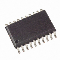
AT90S2313-4SI Atmel, AT90S2313-4SI Datasheet - Page 51

AT90S2313-4SI
Manufacturer Part Number
AT90S2313-4SI
Description
MCU 2K FLASH 4MHZ 20-SOIC
Manufacturer
Atmel
Series
AVR® 90Sr
Datasheet
1.AT90S2313-10PC.pdf
(92 pages)
Specifications of AT90S2313-4SI
Core Processor
AVR
Core Size
8-Bit
Speed
4MHz
Connectivity
SPI, UART/USART
Peripherals
Brown-out Detect/Reset, POR, PWM, WDT
Number Of I /o
15
Program Memory Size
2KB (1K x 16)
Program Memory Type
FLASH
Eeprom Size
128 x 8
Ram Size
128 x 8
Voltage - Supply (vcc/vdd)
2.7 V ~ 6 V
Oscillator Type
External
Operating Temperature
-40°C ~ 85°C
Package / Case
20-SOIC (7.5mm Width)
Data Bus Width
8 bit
Data Ram Size
128 B
Interface Type
SPI, UART
Maximum Clock Frequency
4 MHz
Number Of Programmable I/os
15
Number Of Timers
1 x 8 bit
Operating Supply Voltage
2.7 V to 6 V
Maximum Operating Temperature
+ 85 C
Mounting Style
SMD/SMT
Minimum Operating Temperature
- 40 C
Lead Free Status / RoHS Status
Contains lead / RoHS non-compliant
Data Converters
-
Lead Free Status / Rohs Status
No
Available stocks
Company
Part Number
Manufacturer
Quantity
Price
Part Number:
AT90S2313-4SI
Manufacturer:
ATMEL/爱特梅尔
Quantity:
20 000
Port B as General Digital I/O
Alternate Functions of Port B
0839I–AVR–06/02
The Port B Input Pins address (PINB) is not a register; this address enables access to
the physical value on each Port B pin. When reading PORTB, the Port B Data Latch is
read, and when reading PINB, the logical values present on the pins are read.
All eight pins in Port B have equal functionality when used as digital I/O pins.
PBn, general I/O pin: The DDBn bit in the DDRB Register selects the direction of this
pin. If DDBn is set (one), PBn is configured as an output pin. If DDBn is cleared (zero),
PBn is configured as an input pin. If PORTBn is set (one) when the pin is configured as
an input pin, the MOS pull-up resistor is activated. To switch the pull-up resistor off, the
PORTBn has to be cleared (zero) or the pin has to be configured as an output pin The
Port B pins are tri-stated when a reset condition becomes active, even if the clock is not
active.
Table 18. DDBn Effects on Port B Pins
Note:
The alternate pin functions of Port B are:
• SCK – Port B, Bit 7
SCK, Clock Input pin for memory up/downloading.
• MISO – Port B, Bit 6
MISO, Data Output pin for memory uploading.
• MOSI – Port B, Bit 5
MOSI, Data Input pin for memory downloading.
• OC1 – Port B, Bit 3
OC1, Output Compare Match Output. The PB3 pin can serve as an external output for
Timer1 Compare Match. The PB3 pin has to be configured as an output (DDB3 is set
[one]) to serve this function. See the timer description for further details, and how to
enable the output.
• AIN1 – Port B, Bit 1
AIN1, Analog Comparator Negative Input. When configured as an input (DDB1 is
cleared [zero]) and with the internal MOS pull-up resistor switched off (PB1 is cleared
[zero]), this pin also serves as the negative input of the On-chip Analog Comparator.
• AIN0 – Port B, Bit 0
AIN0, Analog Comparator Positive Input. When configured as an input (DDB0 is cleared
[zero]) and with the internal MOS pull-up resistor switched off (PB0 is cleared [zero]),
this pin also serves as the positive input of the On-chip Analog Comparator.
DDBn
0
0
1
1
1. n: 7, 6…0, pin number.
PORTBn
0
1
0
1
Output
Output
Input
Input
I/O
Pull-up
Yes
No
No
No
(1)
Comment
Tri-state (High-Z)
PBn will source current if ext. pulled low
Push-pull Zero Output
Push-pull One Output
AT90S2313
51


