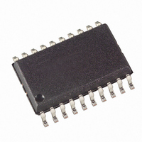
AT90S2313-4SI Atmel, AT90S2313-4SI Datasheet - Page 35

AT90S2313-4SI
Manufacturer Part Number
AT90S2313-4SI
Description
MCU 2K FLASH 4MHZ 20-SOIC
Manufacturer
Atmel
Series
AVR® 90Sr
Datasheet
1.AT90S2313-10PC.pdf
(92 pages)
Specifications of AT90S2313-4SI
Core Processor
AVR
Core Size
8-Bit
Speed
4MHz
Connectivity
SPI, UART/USART
Peripherals
Brown-out Detect/Reset, POR, PWM, WDT
Number Of I /o
15
Program Memory Size
2KB (1K x 16)
Program Memory Type
FLASH
Eeprom Size
128 x 8
Ram Size
128 x 8
Voltage - Supply (vcc/vdd)
2.7 V ~ 6 V
Oscillator Type
External
Operating Temperature
-40°C ~ 85°C
Package / Case
20-SOIC (7.5mm Width)
Data Bus Width
8 bit
Data Ram Size
128 B
Interface Type
SPI, UART
Maximum Clock Frequency
4 MHz
Number Of Programmable I/os
15
Number Of Timers
1 x 8 bit
Operating Supply Voltage
2.7 V to 6 V
Maximum Operating Temperature
+ 85 C
Mounting Style
SMD/SMT
Minimum Operating Temperature
- 40 C
Lead Free Status / RoHS Status
Contains lead / RoHS non-compliant
Data Converters
-
Lead Free Status / Rohs Status
No
Available stocks
Company
Part Number
Manufacturer
Quantity
Price
Part Number:
AT90S2313-4SI
Manufacturer:
ATMEL/爱特梅尔
Quantity:
20 000
Timer/Counter1 in PWM Mode
0839I–AVR–06/02
The TEMP Register is also used when accessing TCNT1 and OCR1A. If the main pro-
gram and interrupt routines perform access to registers using TEMP, interrupts must be
disabled during access from the main program or interrupts if interrupts are re-enabled.
When the PWM mode is selected, Timer/Counter1 and the Output Compare Register1
(OCR1A) form an 8-, 9-, or 10-bit, free-running, glitch-free and phase-correct PWM with
output on the PB3(OC1) pin. Timer/Counter1 acts as an up/down counter, counting up
from $0000 to TOP (see Table 11), where it turns and counts down again to zero before
the cycle is repeated. When the counter value matches the contents of the 8, 9 or 10
least significant bits of OCR1A, the PB3(OC1) pin is set or cleared according to the set-
tings of the COM1A1 and COM1A0 bits in the Timer/Counter1 Control Register
(TCCR1). Refer to Table 12 for details.
Table 11. Timer TOP Values and PWM Frequency
Table 12. Compare1 Mode Select in PWM Mode
Note:
Note that in the PWM mode, the 10 least significant OCR1A bits, when written, are
transferred to a temporary location. They are latched when Timer/Counter1 reaches
TOP. This prevents the occurrence of odd-length PWM pulses (glitches) in the event of
an unsynchronized OCR1A write. See Figure 32 for an example.
Figure 32. Effects on Unsynchronized OCR1 Latching
COM1A1
0
0
1
1
Compare Value changes
PWM Resolution
1. The initial state of the OC1 output line is undefined.
COM1A0
10-bit
8-bit
9-bit
0
1
0
1
Compare Value changes
Effect on OC1
Not connected
Not connected
Cleared on compare match, upcounting. Set on compare match,
down-counting (non-inverted PWM).
Cleared on compare match, downcounting. Set on compare match,
up-counting (inverted PWM).
Timer TOP Value
$03FF(1023)
$00FF (255)
$01FF (511)
(1)
AT90S2313
Frequency
f
f
f
TC1
TC1
TC1
/1022
/2046
/510
35


