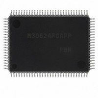
M30624FGAFP#U3 Renesas Electronics America, M30624FGAFP#U3 Datasheet - Page 551

M30624FGAFP#U3
Manufacturer Part Number
M30624FGAFP#U3
Description
IC M16C MCU FLASH 100QFP
Manufacturer
Renesas Electronics America
Series
M16C™ M16C/60r
Datasheets
1.M30622SAFPU5.pdf
(277 pages)
2.M30622SAFPU5.pdf
(617 pages)
3.M30622SAFPU5.pdf
(308 pages)
Specifications of M30624FGAFP#U3
Core Processor
M16C/60
Core Size
16-Bit
Speed
16MHz
Connectivity
SIO, UART/USART
Peripherals
DMA, PWM, WDT
Number Of I /o
85
Program Memory Size
256KB (256K x 8)
Program Memory Type
FLASH
Ram Size
20K x 8
Voltage - Supply (vcc/vdd)
4.2 V ~ 5.5 V
Data Converters
A/D 10x10b, D/A 2x8b
Oscillator Type
Internal
Operating Temperature
-40°C ~ 85°C
Package / Case
100-QFP
For Use With
867-1000 - KIT QUICK START RENESAS 62PM3062PT3-CPE-3 - EMULATOR COMPACT M16C/62P/30P
Lead Free Status / RoHS Status
Lead free / RoHS Compliant
Eeprom Size
-
Available stocks
Company
Part Number
Manufacturer
Quantity
Price
Part Number:
M30624FGAFP#U3M30624FGAFP#D3
Manufacturer:
Renesas Electronics America
Quantity:
10 000
Part Number:
M30624FGAFP#U3M30624FGAFP#D5
Manufacturer:
Renesas Electronics America
Quantity:
10 000
- Current page: 551 of 617
- Download datasheet (9Mb)
External Buses
2-232
4.4 Connectable Memories
4.4.1 Operation Frequency and Access Time
Connectable memories depend upon the BCLK frequency f(BCLK). The frequency of f(BCLK) is equal to
that of the BCLK , and is contingent on the oscillator's frequency and on the settings in the system clock
select bits (bit 6 of address 0006
The following are the conditional equations for the connections. Meet these conditions minimally. Fig-
ures 4.4.1 and 4.4.2 show the relation between the frequency of BCLK and memory.
(1) Read cycle time (tCR)/write cycle time (tCW)
(2) Address access time [ta(A)]
(3) Chip select access time [ta(S)]
Read cycle time (tCR) and write cycle time (tCW) must satisfy the following conditional expressions:
• With the Wait option cleared
• With the Wait option selected
Address access time [ta(A)] must satisfy the following conditional expressions:
(a) Vcc = 5V
• With the Wait option cleared
• With the Wait option selected
(b) Vcc = 3V
• With the Wait option cleared
• With the Wait option selected
Chip select access time [ta(S)] must satisfy the following conditional expressions:
(a) Vcc = 5V
• With the Wait option cleared
• With the Wait option selected
tCR < 10
tCR < 2 X 10
ta(A) < 10
ta(A) < 2 X 10
ta(A) < 10
ta(A) < 2 X10
ta(S) < 10
ta(S) < 2 X10
* 65(ns)
* 140(ns) = td(BCLK-AD) + tsu(DB – RD) – th(BCLK – RD)
* 65(ns)
9
/f(BCLK) and tCW < 10
9
9
9
/f(BCLK) – 65(ns)*
/f(BCLK) – 140(ns)*
/f(BCLK) – 65(ns)*
= td(BCLK – AD) + tsu(DB – RD) – th(BCLK – RD)
= (address output delay time) + (data input setup time) – (RD signal output hold time)
= (address output delay time) + (data input setup time) – (RD signal output hold time)
= td(BCLK – CS) + tsu(DB – RD) – th(BCLK – RD)
= (chip select output delay time) + (data input setup time) – (RD signal output hold time)
9
9
9
/f(BCLK) and tCW < 2 X 10
9
/f(BCLK) – 140(ns)*
/f(BCLK) – 65(ns)*
/f(BCLK) – 65(ns)*
16
, and bits 6 and 7 of address 0007
9
/f(BCLK)
9
/f(BCLK)
SINGLE-CHIP 16-BIT CMOS MICROCOMPUTER
16
).
M16C / 62A Group
Mitsubishi microcomputers
Related parts for M30624FGAFP#U3
Image
Part Number
Description
Manufacturer
Datasheet
Request
R

Part Number:
Description:
KIT STARTER FOR M16C/29
Manufacturer:
Renesas Electronics America
Datasheet:

Part Number:
Description:
KIT STARTER FOR R8C/2D
Manufacturer:
Renesas Electronics America
Datasheet:

Part Number:
Description:
R0K33062P STARTER KIT
Manufacturer:
Renesas Electronics America
Datasheet:

Part Number:
Description:
KIT STARTER FOR R8C/23 E8A
Manufacturer:
Renesas Electronics America
Datasheet:

Part Number:
Description:
KIT STARTER FOR R8C/25
Manufacturer:
Renesas Electronics America
Datasheet:

Part Number:
Description:
KIT STARTER H8S2456 SHARPE DSPLY
Manufacturer:
Renesas Electronics America
Datasheet:

Part Number:
Description:
KIT STARTER FOR R8C38C
Manufacturer:
Renesas Electronics America
Datasheet:

Part Number:
Description:
KIT STARTER FOR R8C35C
Manufacturer:
Renesas Electronics America
Datasheet:

Part Number:
Description:
KIT STARTER FOR R8CL3AC+LCD APPS
Manufacturer:
Renesas Electronics America
Datasheet:

Part Number:
Description:
KIT STARTER FOR RX610
Manufacturer:
Renesas Electronics America
Datasheet:

Part Number:
Description:
KIT STARTER FOR R32C/118
Manufacturer:
Renesas Electronics America
Datasheet:

Part Number:
Description:
KIT DEV RSK-R8C/26-29
Manufacturer:
Renesas Electronics America
Datasheet:

Part Number:
Description:
KIT STARTER FOR SH7124
Manufacturer:
Renesas Electronics America
Datasheet:

Part Number:
Description:
KIT STARTER FOR H8SX/1622
Manufacturer:
Renesas Electronics America
Datasheet:

Part Number:
Description:
KIT DEV FOR SH7203
Manufacturer:
Renesas Electronics America
Datasheet:


