D12363VTE33 Renesas Electronics America, D12363VTE33 Datasheet - Page 231
D12363VTE33
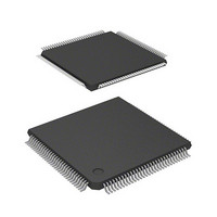
Manufacturer Part Number
D12363VTE33
Description
MCU 3V 0K 120-TQFP
Manufacturer
Renesas Electronics America
Series
H8® H8S/2300r
Datasheet
1.DF2368VTE34V.pdf
(1044 pages)
Specifications of D12363VTE33
Core Processor
H8S/2000
Core Size
16-Bit
Speed
33MHz
Connectivity
I²C, IrDA, SCI, SmartCard
Peripherals
DMA, POR, PWM, WDT
Number Of I /o
84
Program Memory Type
ROMless
Ram Size
16K x 8
Voltage - Supply (vcc/vdd)
3 V ~ 3.6 V
Data Converters
A/D 10x10b, D/A 2x8b
Oscillator Type
Internal
Operating Temperature
-20°C ~ 75°C
Package / Case
120-TQFP, 120-VQFP
Lead Free Status / RoHS Status
Contains lead / RoHS non-compliant
Eeprom Size
-
Program Memory Size
-
Other names
HD6412363VTE33
HD6412363VTE33
HD6412363VTE33
Available stocks
Company
Part Number
Manufacturer
Quantity
Price
Company:

Part Number:
D12363VTE33V
Manufacturer:
Renesas Electronics America
Quantity:
10 000


If a row address hold time or read access time is necessary, making a setting in bits RCD1 and
RCD0 in DRACCR allows from one to three T
to be inserted between the T
the column address is output. Use the setting that gives the optimum row address signal hold time
relative to the falling edge of the RAS signal according to the DRAM connected and the operating
frequency of this LSI. Figure 6.23 shows an example of the timing when one T
Read
Write
Note: n = 2, 3
Figure 6.23 Example of Timing with One Row Address Output Maintenance State
φ
Address bus
RASn (CSn)
UCAS, LCAS
WE (HWR)
OE (RD)
Data bus
WE (HWR)
OE (RD)
Data bus
r
cycle, in which the RAS signal goes low, and the T
T
p
(RAST = 0, CAST = 0)
Row address
T
r
rw
states, in which row address output is maintained,
T
Rev.6.00 Mar. 18, 2009 Page 171 of 980
rw
Section 6 Bus Controller (BSC)
High
High
T
Column address
c1
rw
REJ09B0050-0600
c1
state is set.
cycle, in which
T
c2
Related parts for D12363VTE33
Image
Part Number
Description
Manufacturer
Datasheet
Request
R

Part Number:
Description:
KIT STARTER FOR M16C/29
Manufacturer:
Renesas Electronics America
Datasheet:

Part Number:
Description:
KIT STARTER FOR R8C/2D
Manufacturer:
Renesas Electronics America
Datasheet:

Part Number:
Description:
R0K33062P STARTER KIT
Manufacturer:
Renesas Electronics America
Datasheet:

Part Number:
Description:
KIT STARTER FOR R8C/23 E8A
Manufacturer:
Renesas Electronics America
Datasheet:

Part Number:
Description:
KIT STARTER FOR R8C/25
Manufacturer:
Renesas Electronics America
Datasheet:

Part Number:
Description:
KIT STARTER H8S2456 SHARPE DSPLY
Manufacturer:
Renesas Electronics America
Datasheet:

Part Number:
Description:
KIT STARTER FOR R8C38C
Manufacturer:
Renesas Electronics America
Datasheet:

Part Number:
Description:
KIT STARTER FOR R8C35C
Manufacturer:
Renesas Electronics America
Datasheet:

Part Number:
Description:
KIT STARTER FOR R8CL3AC+LCD APPS
Manufacturer:
Renesas Electronics America
Datasheet:
Part Number:
Description:
KIT STARTER FOR RX610
Manufacturer:
Renesas Electronics America
Datasheet:

Part Number:
Description:
KIT STARTER FOR R32C/118
Manufacturer:
Renesas Electronics America
Datasheet:

Part Number:
Description:
KIT DEV RSK-R8C/26-29
Manufacturer:
Renesas Electronics America
Datasheet:

Part Number:
Description:
KIT STARTER FOR SH7124
Manufacturer:
Renesas Electronics America
Datasheet:

Part Number:
Description:
KIT STARTER FOR H8SX/1622
Manufacturer:
Renesas Electronics America
Datasheet:

Part Number:
Description:
KIT DEV FOR SH7203
Manufacturer:
Renesas Electronics America
Datasheet: